The Future Of Packaging Gets Blurry – Fanouts, ABF, Organic Interposers, Embedded Bridges – Advanced Packaging Part 4
Advanced Packaging Part 4
Advanced packaging is all the rage; for a primer on the topic, read our multi-part series. So far in the series, we have discussed the need for advanced packaging, the various types of advanced packaging offered by firms, and the tool market for thermocompression bonding (TCB), including Intel’s unique use case. This article will be part 4 of that series, digging into the blurring lines of 2.1D, 2.3D, and 2.5D advanced packaging. At IMAPS 2022, many advancements in the field were shown, and the future of the advanced packaging industry is very dynamic. As a short recap, there are currently four main groups of advanced packages.
3D = Active silicon stacked on active silicon – The most well-known forms are AMD’s 3D V-Cache utilizing TSMC’s SoIC CoW and Graphcore’s IPU BOW utilizing TSMC’s SoIC WoW.
2.5D = Active silicon stacked on passive silicon – The most well-known forms are Nvidia AI GPUs with HBM memory utilizing TSMC’s CoWoS-S and Intel Meteor Lake CPUs utilizing Intel’s Foveros.
Fanout RDL (Laminate with epoxy mold compounds) – The most well-known forms are TSMC’s InFO utilized in Apple’s A series, S series, and M series chips, ASE FoCoS, and Amkor WLFO. Panel level is in development from multiple players.
Build-up ABF substrate (copper-core clad with Ajinomoto build-up film layers and RDL layers) – The most well-known forms are Intel and AMD PC and Datacenter chips.
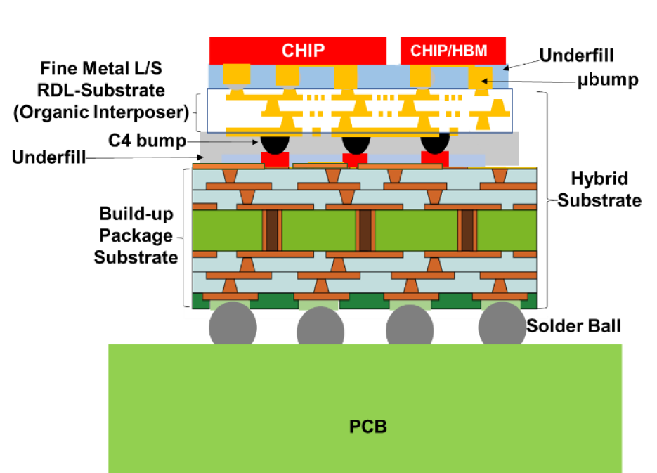
In most cases of advanced packaging, a build-up ABF substrate is still utilized. These are called hybrid substrates.
Another source of ambiguity with advanced packaging is that engineers often use the word organic substrate. Both the ABF and core fanouts contain organic epoxy chemistries.
The categorization across 2.5D to 3D seems simple, but there are many permutations of packaging varieties that blur the lines between 2.3D and 2.1D. Furthermore, as these 2.3D and 2.1D packages advance in capabilities, 2.5D will cede market share.
With Intel’s EMIB, a silicon bridge is placed inside a cavity in a build-up ABF substrate. The primary purpose is to avoid using an expensive silicon interposer and to grow packages beyond the reticle limit. EMIB technically isn’t 2.5D packaging, but it does bring many of the purported benefits. How does it compare to a pure 2.5D silicon interposer or a high-density fanout in cost and performance? The jury is still out on future generations, but the first generation does not compare favorably.
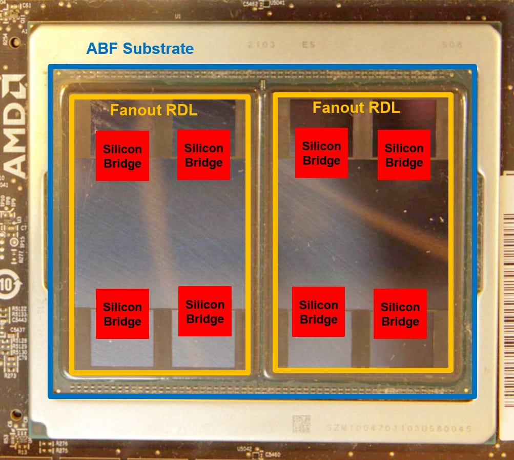
AMD’s MI250X GPU (annotated above) and Apple’s M1 Ultra are examples of multiple types of packaging in one product. Instead of using a silicon interposer to connect the GPU die to the HBM, there are silicon bridges between the GPU die and each HBM. Fanouts with embedded bridges are similar to Intel’s EMIB, but the manufacturing flow is entirely different, fanout RDL vs build-up substrate.
In the case of MI250X, two separate fanout RDL assemblies with the silicon bridges and GPU/HBM are packaged on top of a large ABF substrate.
While costs are theoretically lower with this approach due to minimizing the use of expensive silicon interposers, there is a higher probability of yield loss than with conventional 2.5D silicon interposers.
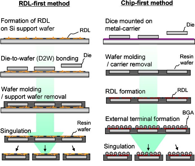
Fanout RDL is not a single process. It can be built with a few different material types. Furthermore, it can be RDL-first or Chip-first flow.
Whether an RDL-first or Chip-first process flow for fanout RDL is utilized, the completed hybrid substrate cannot be tested before dies are placed. Good dies can be lost if the fanout to substrate bonding process. Yield loss is the primary reason silicon interposers continue to be used despite the theoretically lower cost of fanout RDL especially with panel level fanout. These yield issues can extend to substrate warping due to the coefficient of thermal expansion (CTE) mismatch between fanout RDL materials, build-up substrates, and silicon.
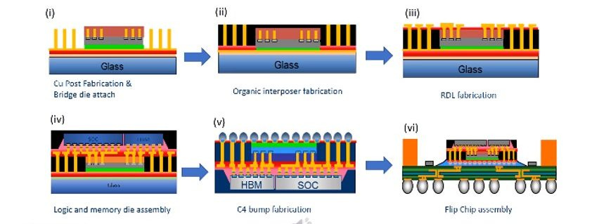
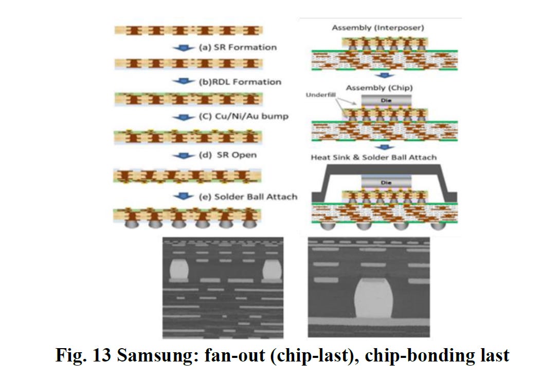
Samsung, Shinko, Unimicron, SPIL, and TSMC have been researching packaging processes where the fanout RDL is fabricated first; then, the fanout RDL is bonded on a build-up ABF substrate. The bonded hybrid substrate is then tested before finally having the chips bonded to it. This is called fanout (RDL-First or Chip-Last), Chip Bonding Last. Each firm has its tweaks, with some using organic or inorganic materials. Higher assembly yields and logistics associated with having known good substrates for advanced packaging presents a huge advantage.
The datacenter and PC industries have traditionally operated with a supply chain that matches known good substrates with known good dies. RDL-First/Chip Last, Chip Bonding Last is the preferred method for packaging if it can be done cost-effectively.
IC integration with fanout (chip-first) process is simpler with lower cost than fan-out (chip-last or RDL-first) processes. The issue is that chip first means more known good die will be lost to packaging yield. As the industry moves to more expensive process technologies, this packaging yield loss continues to dominate most increases in packaging process cost. Furthermore, fanout (chip-last) integration has other advantages, such as larger die sizes, larger package sizes, less die shift issues, and finer metal L/S for the RDLs. L/S is the line space, which refers to the width of the metal interconnects and the space between them.
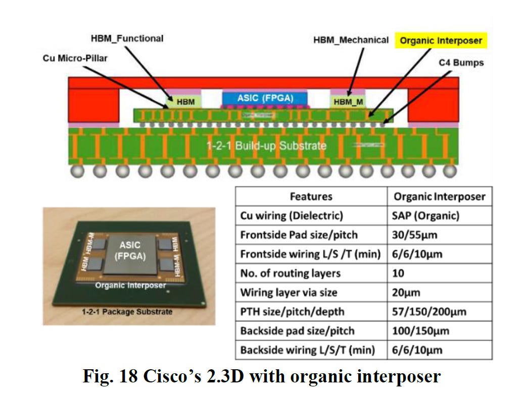
Furthermore, non-fanout technologies are also improving. Cisco has demonstrated research related to coreless organic substrates. The major manufacturing steps for making this organic interposer are the same as those for build-up package substrate, except there is no copper core. Cisco demonstrated 10 routing layers with a denser L/S compared to standard build-up ABF substrates with a core.
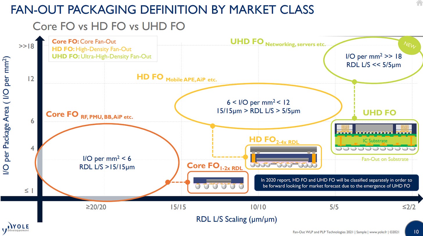
Nowadays, build-up ABF substrates have an L/S as dense as 10-micron; the Cisco research shows the organic substrate going down to 6-micron L/S. The core fanout market has L/S in the 15-micron range. Some advanced fanouts, such as AMD’s RDNA 3 GPUs and a MediaTek network processor, go down to 2-micron L/S. EMIB reaches 5-micron L/S with the first generation and is rumored to reach 2-micron L/S with future generations.
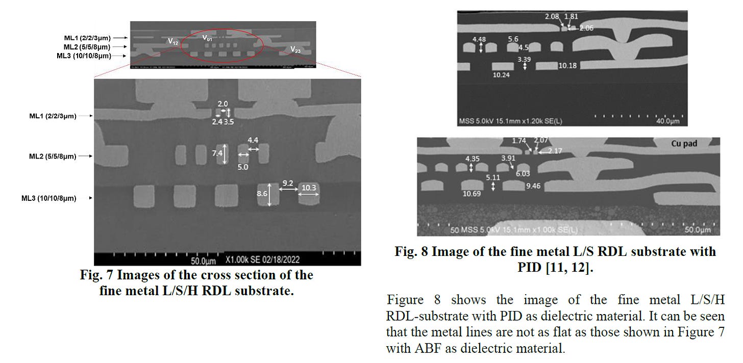
The core fanout and HD fanout market is getting somewhat cannibalized outside of mobile applications as build-up ABF substrates improve. Regarding dielectric materials, photo-imageable dielectrics (PID) are currently able to reach finer pitches. Despite this, ABF has many advantages regarding surface variation, as shown by Unimicron.
Unimicorn looks to stick with a modified ABF as that is their core competency. Fine-pitch coreless ABF sticks with its existing business model of delivering known good (hybrid) substrates. They can achieve a 3-micron L/S with better surface variation, which allows scaling to higher layer counts. Their coreless ABF substrate could be very competitive with current advanced fanouts. It is done on panels, so competitive with wafer level and approaching future panel fanouts. While it is limited to 3 RDL layers, the path to scaling to more layers is easier than that of fanout RDL.
The coreless ABF substrate is thicker, which can be an issue for mobile applications, but the reliability and performance should be better for high-performance applications.
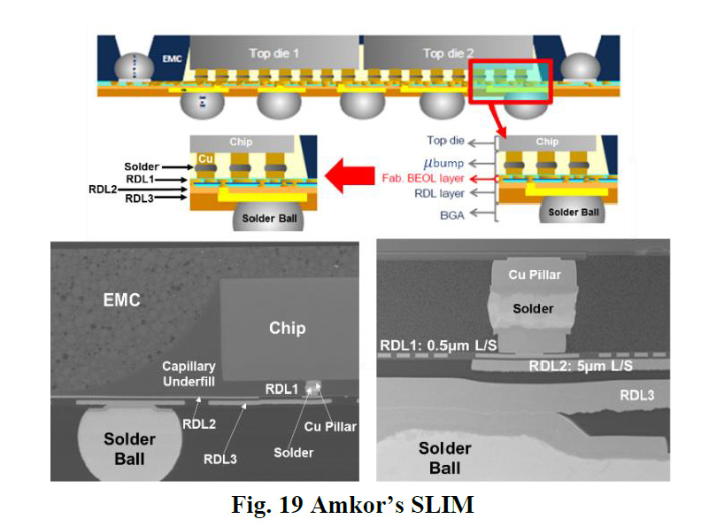
When chasing L/S, Amkor SLIM and ASE SPIL NTI can achieve 0.4-micron and 0.5-micron. Both are limited to these fine pitches on only the first layer.
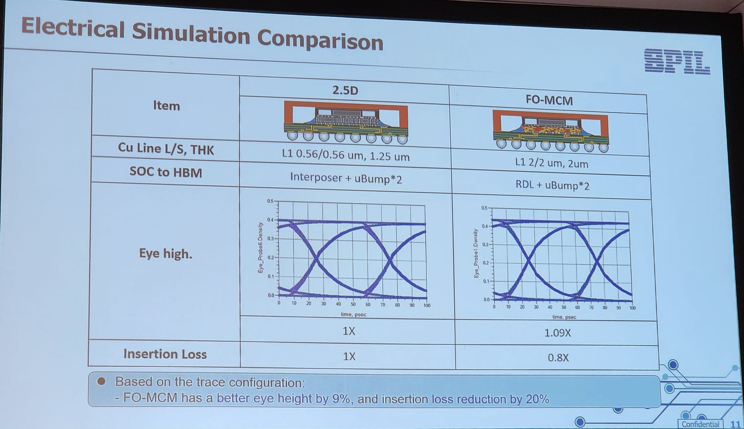
ASE SPIL presented their fanout RDL as more performant than a 2.5D advanced package for connecting HBM dies to a SOC. ASE SPIL claimed a better eye height and less loss reduction, allowing higher signaling rates with less noise through the package.
While build-up ABF substrates will remain the base of the advanced packaging market, they are moving up in performance and density with the transition to coreless substrates. Furthermore, these ABF-based substrates can reach higher layer counts, as shown by Cisco, due to the superior surface variation characteristics shown by Unimicron. ABF substrates are catching up and surpassing fanout RDLs for many use cases.
Costs and yields are also essential factors as RDL fanouts are moving up into applications previously occupied by only 2.5D interposers. Fanout processes with silicon bridges are beginning to ramp, but new processes integrating ASICs with HBM without the use of silicon bridges are also coming closer to production. These advancements in fanouts and ABF substrates are rapidly blurring the lines between advanced packages.
There are multiple variables to consider when evaluating advanced IC packages in the 2.1D to 2.5D realm. Pad pitch, L/S, and layer counts are essential factors, but reliability, warpage concerns, package cost, yields, and package sizes are also under consideration. In the future, a hybrid substrate with a coreless ABF substrate packaged on top of a standard build-up ABF substrate may be the best choice for some use cases. In other cases, a chip-first Fanout RDL packaged on top of a standard build-up ABF substrate could be the best choice for another use case. The tradeoffs involved with packaging are becoming more challenging to evaluate with heterogeneous integration diversity in the number and types of dies.





Great summary! I'd like to read other articles in that topic. :)
Yeah. But you talk about it somewhat in the article about Austria’s companies