The Gaps In The New China Lithography Restrictions – ASML, SMEE, Nikon, Canon, EUV, DUV, ArFi, ArF Dry, KrF, and Photoresist
The economic cold war rages on. Decades of state-sponsored corporate espionage, hacking, dumping, and draconian restrictions including forced tech transfers for market access from China have led to retaliatory sanctions on China’s access to the 21st century’s most important industry, semiconductors. In October, the US imposed restrictions on AI chips and semiconductor manufacturing equipment, but it did not fully address all concerns.
Over the last few months, a few of these were partially addressed, but they haven’t closed the biggest gaps. The US is the leader in wafer fabrication equipment with a majority share in deposition, etch, process control, CMP, and ion implantation, but many US equipment makers, such as Applied Materials, Lam Research, and KLA, have complained that US restrictions would allow overseas competitors such as the Dutch ASM International and Japanese Tokyo Electron to gain market share and blunt the impact of the technology restrictions.
Furthermore, the world’s largest equipment maker, ASML, has been dogmatic about not following US technology restrictions.
As a European-based company with limited US technology in our systems, ASML can continue to ship all non-EUV lithography systems to China out of the Netherlands.
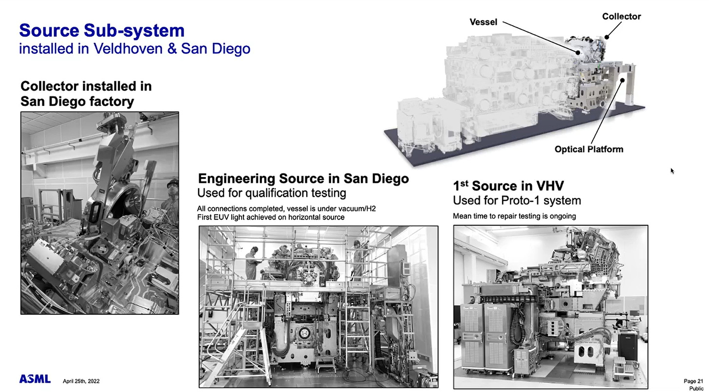
This is despite ASML’s source engineering being done in San Diego by a US company they acquired, Cymer.
Furthermore, mask-related and OPC software required to operate lithography tools is also engineered in the US. While the US certainly has options to make ASML comply with technology restrictions due to its high US-based technology content, the US has chosen the diplomatic route.
The US, Japan, and the Netherlands have been hosting discussions to restrict China’s access to lithography equipment over the last few months. On Friday, news broke that the three countries agreed to certain restrictions on lithography equipment. The question remains, how far do these restrictions go, and what do they contain? Our understanding is that these restrictions are extremely limited and only regard ArFi tools. This agreement is still verbal in nature, but we believe the 3 countries have agree to move forward on this basis. Some other non-lithography tools are also supposedly included. Today we are going to discuss the many gaping holes in the newly agreed lithography restrictions regarding equipment, chemicals, and component supply chains.
Equipment Supply Chain
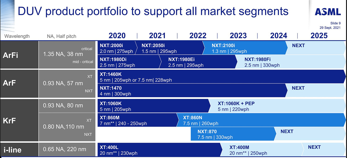
The primary avenue to restrict China’s access to semiconductors is with equipment. While there is a tri-lateral agreement for blocking access to DUV lithography, there is no mention of how far back this goes. DUV is a very broad technology that includes Krypton fluoride (KrF), Argon Fluoride (ArF), and Argon Fluoride Immersion (ArFi) lithography.
Nikon released the first DUV tool called NSR-1505EX in 1988 using KrF lithography. It initially had a resolution of 500nm, but over time it was upgraded to be capable of 250nm with an overlay of 100nm. The newly agreed restrictions by the US, Netherlands, and Japan does not cover technology this old. On the other hand, ASML’s NXT 2100i, released in 2022, has an overlay of 1.5nm and can pattern the minimum features required for advanced nodes.
If the goal is to prevent China from acquiring 14nm, 7nm, or 5nm process technologies, then the ban must reach a differing level of tooling capable of processing the features for these nodes. For example, TSMC’s 16nm and 12nm process technologies have a minimum metal pitch of 64nm. TSMC’s 7nm process technology has a minimum metal pitch of 40nm. TSMC’s 5nm process technology has a minimum metal pitch of 28nm.
Any ban on lithography equipment must consider these minimum metal pitches as the specifications for banning equipment.
In the Rayleigh criterion equation (CD = k1 • λ / NA), the CD is the critical dimension, the smallest possible feature size. λ is the wavelength of light used. NA is the numerical aperture of the optics, defining how much light they can collect. Finally, k1 (or the k1 factor) is a coefficient that depends on many factors related to the chip manufacturing process. The physical limit lithography is k1 = 0.25.
Self-aligned quad patterning (SAQP) is generally considered the furthest economic way to stretch a DUV lithography generation. While there are more complex schemes for lithography, we will stick to what is economically feasible today. TSMC and China’s SMIC have achieved 7nm process technology, without EUV, using SAQP with argon fluoride immersion (ArFi) lithography, but that isn’t the limit of what’s economically achievable.
The 28nm minimum metal pitch used on TSMC’s N5 could be manufactured without EUV. SAQP using ArFi lithography (NA=1.35, λ=193nm) can produce this feature size at a k1 of 0.391. If the goal is to stop China from achieving 5nm process technology, then ArFi shipments must be blocked. ASML and Nikon can manufacture ArFi lithography tools capable of 28nm minimum metal pitch. While this wouldn’t be as cost-effective as EUV, the delta would not be unachievable for a nation-state like China.
If the goal is to prevent China from achieving high volume 7nm process technology, then all tools that can achieve a 40nm minimum metal pitch used on TSMC 7nm class process technologies must be blocked. The new restrictions would include ArFi lithography, but they would also need to extend further. SAQP using dry argon fluoride ArF lithography (NA=0.93, λ=193nm) can produce this feature size with a k1 of 0.385. Again, this isn’t going to be as economical as Intel, TSMC, and SMIC’s ArFi DUV “7nm,” but it is achievable, especially given the importance of national security. The cost delta would be significantly less than that of the subsidies for a nuclear power plant in the US.
If the goal is to prevent China from expanding their high volume 14nm process technology, then all tools that can achieve a minimum metal pitch of 64nm used on nodes, such as TSMC’s 16nm and 12nm and Samsung’s 14nm, must be blocked. Not only should these restrictions, if adequately enforced, include ArF lithography tools, but they would also need to extend further to some types of Krypton fluoride (KrF) tools. Krypton fluoride has a λ=248nm, but there were multiple generations of the lens stack. In each generation, NA improved from 0.6 to 0.8 to 0.93.
SAQP using the most advanced KrF lithography (NA=0.93, λ=248nm), can produce this feature size with a k1 of 0.48. SAQP using the mid-range KrF lithography (NA=0.8, λ=248nm), can create this feature size with a k1 of 0.413. These are very achievable with tools from ASML, Nikon, or Canon. Again, the economics here would not be optimal, but even doubling lithography costs on a 14nm class node would only lead to a ~19% increase in cost for each wafer. This is already economically viable with the level of state subsidies China gives their domestic firms.
We should note that regulators should also look to the overlay specification when determining which tools to restrict. In lithography, overlay refers to the alignment accuracy between different layers during manufacturing. It is the positional accuracy with which one layer is aligned to another layer. Each of our examples utilized self-aligned quad patterning (SAQP), meaning 4-layers of lithography need to be aligned. As such, overlay control is critical.
ASML’s most advanced EUV steppers have an overlay accuracy of 1.1nm. The prior version, 3400C, which was the primary EUV tool they shipped in 2021, has an overlay accuracy of 1.5nm. This is worse than ASML’s most advanced DUV tool, 2100i. For today, we won’t dive too much into where we believe the line for overlay accuracy on 14nm, 7nm, and 5nm sits for export controls, as that would be far too much into the weeds for most readers.
Chemical Supply Chain
The next gap in the new export controls is the chemical supply chain, namely photoresist. We did a deep dive into photoresist here, but the summary is that lithography tools require photoresists to pattern features on a wafer. The vast majority of the world’s photoresist is manufactured by a handful of Japanese companies, with the US-based Dupont as the distant 4th place competitor. Photoresist chemical compositions involved a lot of fine-tuning with end customers for the type of lithography, process nodes, types of features, and feature sizes in many cases. Furthermore, the equipment used to deposit, develop, and bake photoresist is also entirely Japanese.
Any country in the world could be blocked from all lithography and, therefore, semiconductor manufacturing if Japan restricted photoresist shipments. The complete lack of restrictions around photoresists represents a significant hole that governmental regulations have not contemplated.
There are over a hundred DUV tools already at SMIC alone. These could be reorganized and shifted to fabricate for different process nodes. SMIC could achieve a capacity of well over 100,000 wafers a month of 7nm foundry capacity with their existing DUV tools alone. This is higher than Samsung and Intel’s advanced node (<=7nm) foundry capacity, combined. If all DUV tools at various Chinese nationals such as HuaHong, Shanghai Huali, YMTC, CXMT, GTA Semi, Nexchip, Yandong, Nexperia, CR Micro, Sien, Fulsemi, SEMC, NSEMI were reappropriated by SMIC, the 7nm capacity they could build would far exceed that of even TSMC’s 7nm.
It is not enough to only block the shipment of new tools to China if the goal is to limit their manufacture of advanced semiconductors. Shipment of photoresists must also be stopped as Western governments do not know what process node existing DUV tools are being used.
Component Supply Chain
This leads to the final gap, the component supply chain. DUV tools must be regularly serviced with replacement parts by ASML, Nikon, and Canon. The service of these tools must also be blocked if the goal is to contain China’s capacity on leading-edge nodes.
While China’s lithography champion, SMEE, is on the sanctions list, SMEE has already shipped working I-Line lithography tools. Their argon fluoride DUV lithography is still not production ready for front-end wafer fabrication. This doesn’t mean they cannot catch up. Many firms in ASML’s lithography supply chain, such as Zeiss, continue to expand in China with joint ventures and technology transfers. Given the civil-military fusion of China, it would be straightforward for these technologies to slip through the cracks into SMEE’s control.
Lastly, mask related tools also have zero restrictions, which is also a hole.
The lack of upstream component supply chain restrictions is a significant hole in the trilateral agreement between the US, Japan, and Netherlands. If the goal is to restrict 5nm, 7nm, and 14nm process technologies, KrF and ArF lithograph equipment, photoresist, and subcomponents must all be limited, or else China will be able to reconfigure existing equipment and accelerate domestic development of lithography tools.


Good note. Thank you.
There is no long term vision for the sanctions. Do we really think with all the scientists and engineers that China has and will have, they won't be producing all these tools? 2 years ago we didn't imagine they would be producing chips at 7nm. I suspect they've been working on them for several years already.
If they start building these tools, western supply chain will be devastated.