ASML & The Semiconductor Market In 2025 & 2030
A critical look at ASML's long term projections and assumptions
ASML just hosted its annual investor day. Included in the day were many claims about the business, technology, and the semiconductor industry. If you want to learn about lithography, check out this article and the Asianometry YouTube channel. This report assumes you understand these topics. The report will discuss semiconductor industry growth by subsegment, including Smartphones, PCs, Consumer Electronics, Wired/Wireless, Datacenter, Automotive, and Industrial Electronics.
Furthermore, we will dive into wafer capacity additions across various process technologies and industries. We will also dive into capacity additions across advanced logic (<28nm), DRAM, NAND, and mature logic (>28nm). The discussion will include semiconductor capital intensity, geopolitical competition, and the regionalization of the semiconductor supply chain. We also discuss the boom in designs and die sizes.
One of the most critically important discussions is around the total wafer fabrication equipment market and lithography intensity through the decade, including the possible impacts of transitions to gate-all-around transistors and 3D DRAM.
Riddled throughout this report, we poke some holes in the 1st party information that ASML provided. As always, 1st party equipment information is baked full of information and assumptions that are very favorable if not straight-up incorrect, as we laid out in this report from June.
Most of the investor community’s sell-side (besides Redburn) just plugged in ASML’s 2025 and 2030 guidance, accounted for buybacks, and said it was at a fair valuation. We want to take a different view and examine ASML from a first principal basis.
To start with, it’s interesting to see ASML on the side of Moore’s Law continuing to be alive, even as so many others rush to call it dead, most notably, Jensen Huang, CEO of Nvidia.
But it's the value of Moore's Law, which is basically reducing the cost per function that will drive our business, and we'll create these building blocks for growth and for solving some of humanity's biggest challenges. And we are a strong believer in this.
Peter Wennink, CEO of ASML
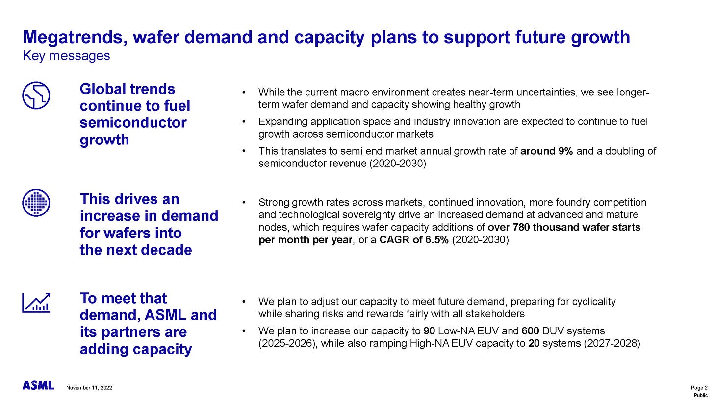
ASML shared that they believe the semiconductor end market will grow at a rate of ~9% annually from 2020 to 2030. For those keeping track, this would mean semiconductor sales in 2025 would exceed $700B, and 2030 would reach ~1.1 Trillion! Compare this to Tech Insights at $1T, McKinsey at $1.1T, and Semi at $1.3T. The highlights are that wafer capacity grows by 780k wafer starts per month (WPM) at a CAGR of 6.5%.
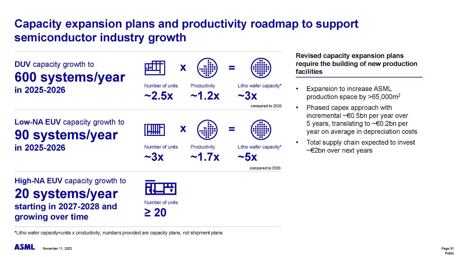
This implies a continuous increase in wafer price increases throughout the decade, which is expected as leading edge and memory wafer prices continue to increase, and density increases peter out relatively. ASML wants to ramp capacity up to 600 DUV tools and 90 EUV tools by 2025. ASML also plans for 20 High-NA EUV tools by 2027/2028. To be clear, this is the capacity target; it is doubtful that ASML will be able to ship this many tools or that the demand is even there.
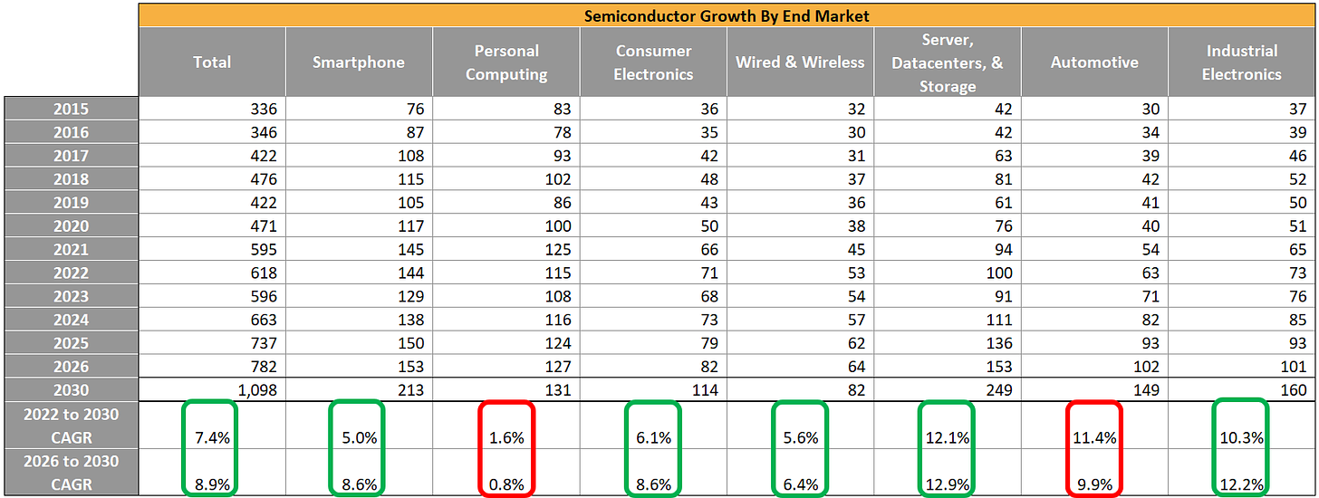
ASML also shared this slide with CAGR data by subsegment by year. We transposed that data into the table below. We calculated the CAGR from 2022 to 2030 and compared that to the CAGR from 2026 to 2030. The interesting detail that can be parsed is that ASML sees most of these segments accelerating in the latter half of the decade except for personal computing and automotive, which they see as having decelerating growth.
ASML went on to fluff on about all the megatrends, cloud, artificial intelligence, green energy, and the transformation to renewable, but there wasn't too much new or interesting content in that section, but there are a few anecdotes.
Some data that we got from some of our customers and some of other companies that is from Shell. It is an estimate that 1 megawatt of wind power will take EUR 3,000 worth of semiconductors and solar EUR 4,000. Now the question. What was the electricity needed in the world in 2019?
It was about 24,000 terawatt hour. Now you can then calculate this and take the average of wind and solar. All the electricity you need in the world, which, of course, is not going to be the case, but it's going to be wind and solar. You come to significant numbers. Now the 24,000 was 21,000 3 years earlier, it was 2019, the 24,000.
Peter Wennink, CEO of ASML
Edit: corrected the math in this section
24,000TWh a year = 24,000,000,000MWh a year
1000 GW of panels produces roughly 1000 TWh of electricity per year given usage rates - you need 24,000 GW (24,000,000MW) of panels in total
24,000,000MWh * €3,000 = €72,000,000,000
24,000,000,000 * €4,000 = €96,000,000,000
100 Billion Euros! And that's assuming max power generation from the solar or wind. These figures include the disparity between average power generation vs peak mismatch.
Now let's say the world goes from it's current 10.7% solar/wind to 50% by the end of the decade, an inrease of 5x, way beyond any credible estimates.
€100B * 40% / 8 years = €5B a year semi
Not that ridiculous, but if we stack on battery storage, the numbers would continue to go even higher.
We did want to share one particular quote from the 65-year-old CEO, which made us groan.
I'm from a generation where actually, we were given the promise of the global village. And I had a discussion with the some young people that actually said, you guys screwed up your generation because you left us with all these problems.
So listen, but our generation did create a global village. Our generation, my generation did create the Internet, did create global travel.
Peter Wennink, ASML’s CEO
It’s interesting to hear that the baby boomer generation invented boats, airplanes, and an internet that doesn't have a massive firewall between China and the rest of the world. Sorry for the aside, folks; back to semiconductors!
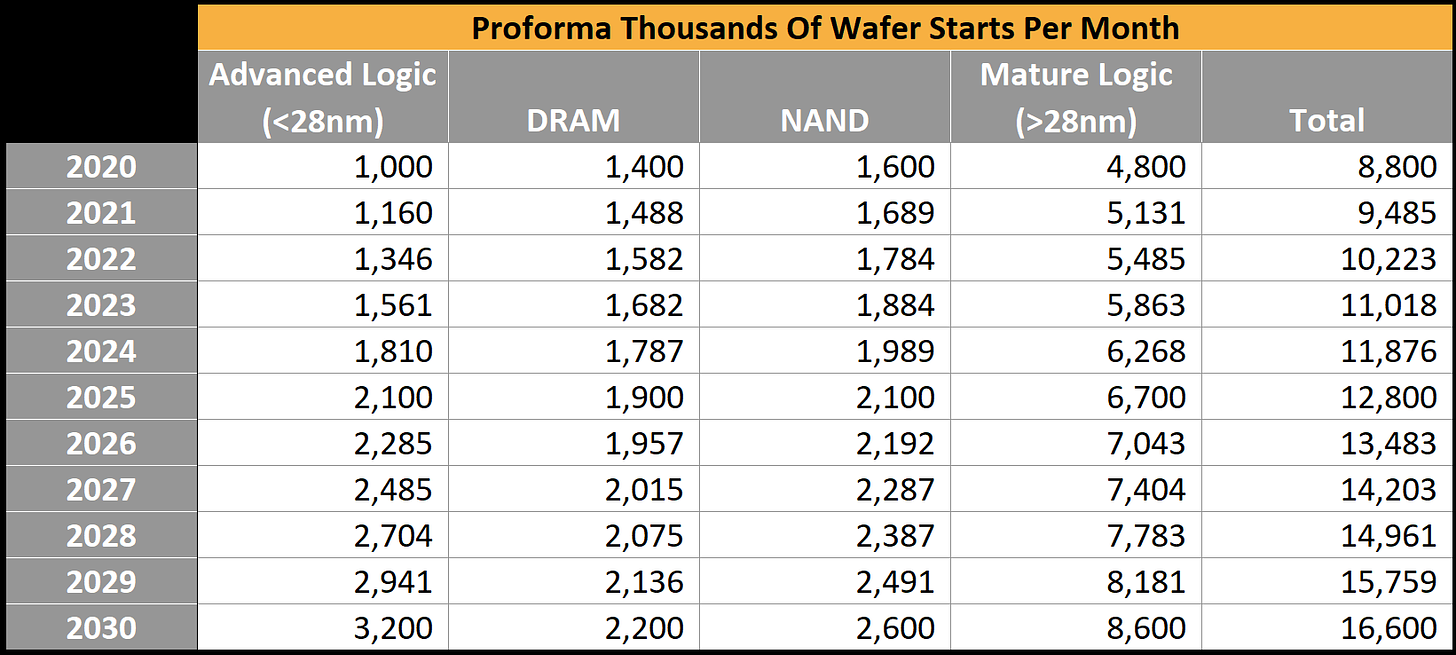
Next up was wafer starts per month by process technology group. We directly transposed ASML’s data, and added the actual CAGR’s given.
Using ASML’s data, we get this curve for wafer starts per month by year. The wafer starts in this table are incorrect, given that we just applied ASML’s CAGR in a straight line. The actual numbers will be much lumpier.
For more clarity on our estimated wafer starts per month, see this piece from a couple of months ago, where we called out Capex cuts and utilization rate issues, including 7nm utilization issues at TSMC and the complete reconfiguring of the Kaohsiung Taiwan fab before others.
The internal SemiAnalysis figures further breakdowns wafer capacity by node, and we see a massive drop in utilization rates occurring now and accelerating in the first half of 2023.
To be clear, ASML thinks the same, although not to the same degree as us. Furthermore, ASML believes there is such a drastic shortage of lithography tools in 2023, so industry weakness will only affect them a little. While there is some shortage of KrF, i-line, ArF, ArFi, and EUV tools, these markets will be satiated in 2023.
ASML argues that the top 50 technology companies, whose entire business is built off running on semiconductors, have $688B in EBIT. These businesses can cede some margin to the semiconductor industry and, ultimately, the tool companies to support a massive capacity build-out.
In February, we wrote about the regionalization of semiconductors due to global supply chain instability. In essence, the deglobalization of semiconductors goes beyond the ruthless economics that has ruled this industry for decades.
The increasing global tensions mean countries will subsidize and build out significant capacity. They have to; there is no choice.
Note that ASML’s chart is very misleading. China’s national government tax subsidies total over $150B for the semiconductor industry. The local subsidies are larger than China’s big fund as well. Furthermore, the big fund has a 5 to 1 investment ratio mandate for private market contributions versus the national government contributions mandate. The big fund’s dollars often exceed that mark. In contrast, we believe the CHIPS Act is likely only to reach a 4.2 to 1.
Our analysis indicates that the CHIPS Act will only boost the US from the current 10.5% of worldwide semiconductor manufacturing value up to 13% to 14% by 2026. That's accounting for Apple moving some production to TSMC Arizona and AMD’s Lisa Su telling us the same. Meanwhile, China will easily exceed 20% of worldwide semiconductor manufacturing in the same time frame.
The technological sovereignty argument is a big part of ASML’s capacity aspirations. ASML believes that an additional 10% capacity will be added each year for technological sovereignty and geographic competition.
This 10% capacity is due to the inherent inefficiencies of a regionalized versus centralized semiconductor fabrication market. This 10% inefficient capacity represents 150 thousand wafers per month added annually.
The first implication from regionalization is there will be a movement towards smaller fabs away from larger giga-fabs. A giga-fab is one that has a monthly production capacity more than 100,000 wafers per month. We can see this already with TSMC’s current investments in Japan, US, and China. These fabs are smaller than their giga-fabs in Taiwan and likely that means they are less efficient. Larger fabs are run more efficiently than many small fabs due to the nature of the incredibly complicated multivariate calculus that involves tool positions, cycle times, throughput per tool, variance in time between tools, the wafer highway that transports wafers across the fab, and much more. A larger fab is better able to balance these factors and therefore extract more throughput out of each tool. These multiple small fabs could have just as many tools, but their output would be lower. Regionalization has a direct impact on the capital intensity of a fab (a measure of revenue versus spending on building the fab).
The second implication is that less efficient operators would be rewarded. Integrated design manufactures such as Intel, Samsung, Texas Instruments, STMicroelectronics, Infineon, and NXP are generally considered to be less efficient at getting wafers through the fab and maximizing utilization of their tools versus foundries. Capital intensity will continue to rise across the industry due to this. Intel states they will run at a long term capital intensity of ~30% with the net capital intensity being 25%. Texas Instruments, a Wall Street darling due to their consistently large buybacks, has stated their long term capital intensity is rising from 6% to 10%.
Dylan Patel, Chief Analyst of SemiAnalysis in “I, Semiconductor – The Regionalization Of Semiconductors Due To Global Supply Chain Instability”
For the record, WFE intensity is artificially high in 2021/2022, and it will fall slightly as the decade progresses, but it will be higher than in the late 2010s. Furthermore, this paradigm of excess capacity due to regionalization also means that utilization rates would fall. Geographically dispersed competing fabs will have to compete on pricing to fill the overbuilt fabs. The combination of factors results in fabrication margins falling.
And if there were any questions about where ASML stands on the current geopolitical mess…
I think the energy transition is something that surprised us for the last couple of -- and there is anecdotal evidence, we had a Chinese customer that actually was in our offices at the beginning of the year, and has said, basically, they were making very mature stuff. It was in power, in some analog products.
And actually said, Peter, we need your help because we're going to build a 300-millimeter fab, 90 nanometers, 9-0.
ASML’s answer is that they will teach China everything they can. This will destroy the profitability of the power semiconductor market for Infineon, ST Micro, and other European companies. 90nm is where the 200mm to 300mm fab transition started. This would lead to the new 90nm 300mm fab having better unit economics than the 90nm 200mm fab despite massive depreciation differences.
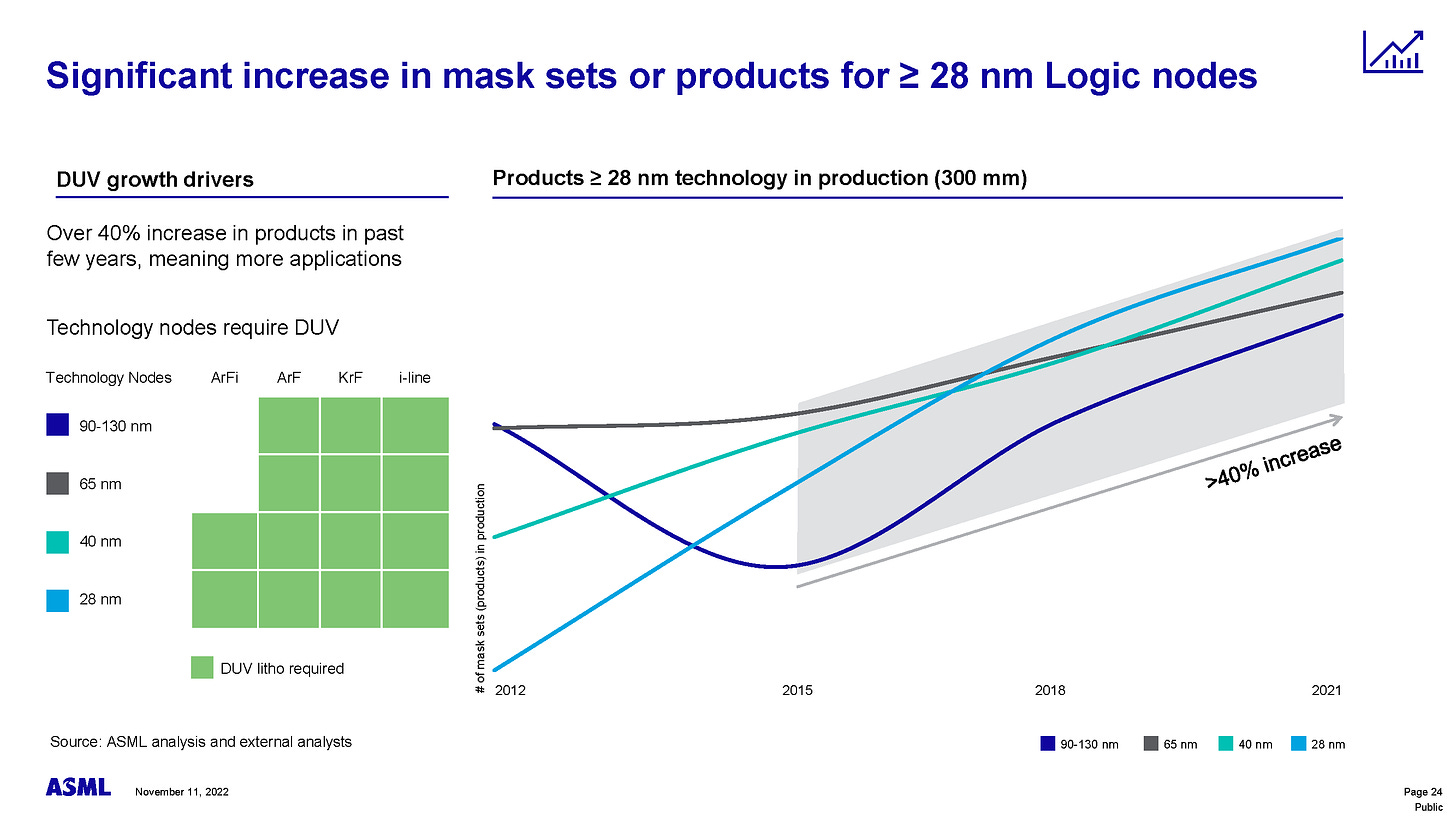
One of the most exciting pieces of data that ASML shared was that the number of mask sets on >28nm increased by 40%. This number is less than the eBeam Initiative’s survey, which indicates 48%, which was presented at the SPIE Advanced Lithography + Patterning conference. Regardless, you can think of that as 40%+ more designs on each trailing edge node. It’s not just more old chips. It’s new designs on mature process technologies.
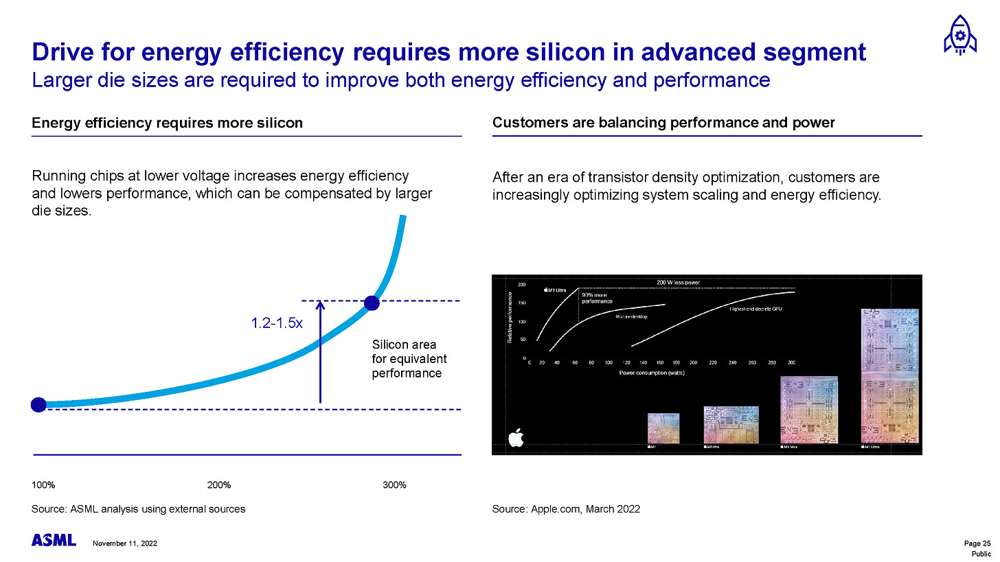
As Moore’s Law slows, die sizes are ballooning. In most cases, ignoring idle power and leakage concerns, a larger, more costly design at lower clocks will produce significantly higher performance per watt. Most architects will tell you that more areas are the simplest solution to achieving power and performance targets. This means that micro-architecture matters more and more for the industry’s economics. We can see this area tradeoff everywhere, from smartphone chips like Qualcomm with their Adreno GPUs in S8G1+ vs. S8G2 to datacenter server CPUs like AMD Genoa and Intel Sapphire Rapids to networking chips from Nvidia, Intel, Marvell, Cisco, and Broadcom.
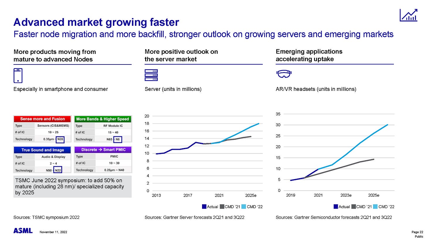
One interesting note is that ASML still has server units up in 2022 and 2023. They should read our 2023 datacenter outlook, where we discuss revenue, ASP, unit volume, and market share by architecture and company because unit volumes are not looking pretty in H2 2022 and 2023.
The other noteworthy thing is that they have increased their estimate for VR/AR mostly off the backs of Meta subsidizing the crap out of the Quest 2. The Quest Pro is a flop, and we hear the Quest 3 will not be subsidized nearly as much. The upcoming Apple device is costly, so we doubt it will move that many millions of units to make up for Meta.
AR will be as big as the smartphone industry one day, and we can’t wait to have the world’s information projected directly into our eyeballs, but that world isn’t coming any time soon.
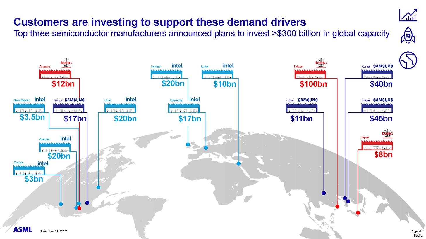
This chart from ASML needs to be clarified because they are counting fabs willy-nilly. SemiAnalysis tracks every project and has over 130 semiconductor manufacturing sites currently being tracked. The $100B of TSMC in Taiwan is a multi-site Capex for multiple years. This should be broken out. The Samsung numbers make no sense. In Korea, P3 is complete and P4 is about to start, but no S7 or V2. So where is the 2nd fab coming from? The Samsung fab in China is also confusing, given that Xi’an is complete and in maintenance/steady upgrade mode. With Intel, Ireland is €13B, which is not $20B; Oregon D1X Mod 3 is larger than what they have listed there. Overall, we give it a 4 out of 10. They should have just listed the total investment sizes at each site to get investors even more excited. In that case, there would be multiple $100B sites, which is more eye-popping for investors.
Lastly, we want to discuss how ASML is rolling this up to their capacity figures. They are accounting for the number of units * productivity improvements to reach a total litho capacity increase of 3x for DUV and 5x for EUV compared to 2020. The productivity increases on the EUV side are pretty significant. The source power increases, and improvements in photoresists such as MOR and dry resist are powering this increase in productivity.
ASML expects its revenue to reach $44B to $60B by 2030. This would mean that the total wafer fabrication equipment market is more like $150B to $280B. That is a massive increase. The range is quite large and could be even larger here, to be fair, given that service is also included in these figures. The main discussion point here is not even the size of the WFE market but lithography intensity at future nodes. IMEC processes can be used to estimate 3nm, 2nm, and 1.4nm lithography intensity.
We believe ASML is a bit hopeful here on their intensity, especially on the future gate-all-around nanosheet nodes. Furthermore, they are entirely discounting 3D DRAM, which is chugging along in the R&D phase at an incredible pace at Samsung and, to some extent SK Hynix. These topics are far too long, and we will discuss them in another note for paid subscribers.





The main concern I have with ASML is that they're largely a play on Moore's law, which is slowing down, and could come to a halt in the coming decade - you can't scale smaller than the size of an atom. For each new node that TSMC and the likes move to, they need to buy more and more ASML tools, especially EUV, to enable this shrinkage. However, once that growth driver levels off, demand for ASML tools will shrink. The company's tools are actually so good that each one they've sold is still in operation! This is great, but not from a business perspective. I bought a huge chunk of ASML in '16 and sold it in the tech bubble of '21. But definitely a great company.
Thanks for an insightful article! Not sure if you got any feedback regarding the the power data?
Anyway, I got curious about it to so did some quick calculations.... Wennink mentioned 24 000 terrawatt hours (TWh) of electricity - which would be the total of energy consumed that year.
To get to the capacity needed to produce that amount, you take the total amount of hours per year (24x365=8760) and then the "efficiency rate" of each power generation technology - wind or solar - and then you can calculate the capacity needed to produce.
So if we use a global average - i.e. wind 26% and solar 14% (average global efficiency data calculated from numbers on capacity and production I found in "Our world in data")
- Assuming that ALL that 24000TWh of energy would be produced from wind it would imply an semis content of roughly EUR 32 bn and if all was solar - EUR 78 bn....