Samsung has long hyped their 3nm process node. They hail it as the first usage of Gate All Around FET in the industry for a commercial process technology. Being first to change transistor architecture is a very coveted prize in the semiconductor world. Intel was the first with their 22nm Tri-Gate technology which made the move from planar FET transistors to FinFET. Samsung wants to take this crown for GAAFET. Despite a lot of marketing and hype building around this node, it looks more and more grim, as the 3nm node is now looking like it is delayed to 2024 for commercial foundry partners.
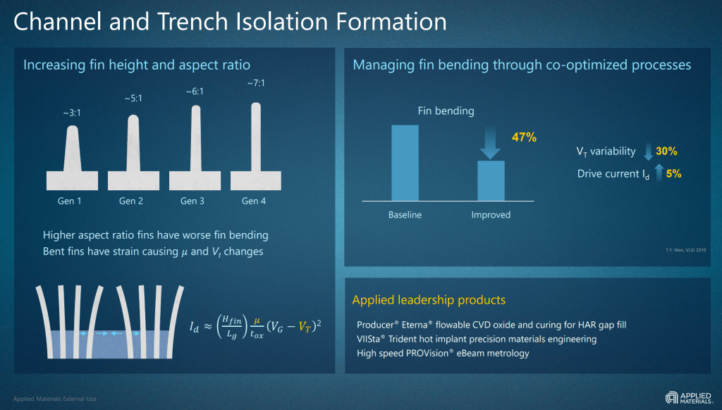
In the last few generations of FinFET, the power scaling has been accomplished by what is known as fin reduction. We have gone from four fin devices to three fin devices to two fins per transistor. In addition, these fins have gotten taller to increase contact area between the channel and gate. These methods of scaling are running out of steam, and without the usage of exotic materials such as Co contacts and SiGe for the channel, it would already be close to over. Taller and fewer fins also come with other issues, which necessitates the next step forward in transistor architecture.
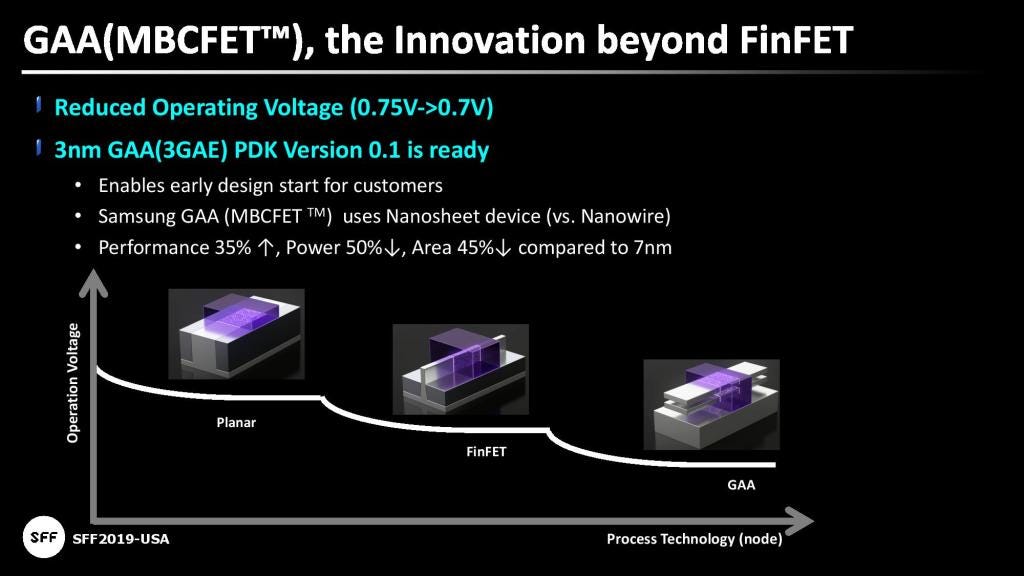
TSMC’s lead in process technology has been growing rapidly. Without a moonshot project, Samsung stand no chance versus the relentless execution from TSMC. In early 2019, they announced the 3GAE process node alongside an early product design kit (PDK) for this technology. Their 3GAE process technology would utilize a MBCFET architecture. Essentially a MBCFET is like turning the fin from FinFET on its side and then stacking the horizontal fins on top of each other. The contact area between the channel and the gate increases dramatically which allows huge gains to power and performance.
Samsung claimed impressive gains with a 35% increase to performance, 50% the power, and 45% the area compared to their 7nm technology. At this event in early 2019, Samsung also claimed their 3GAE process would offer first customer tape outs in 2020, with risk production in late 2020 and volume manufacturing in late 2021.
Fast-forward to 2021 and there are no foundry tape outs and volume production is not anywhere close to delivery. Goals for the process may also seem to have been revised heavily with the comparison to 7nm FinFET going from a 35% performance to 10%. The logic area reduction has gone from 45% to 25%, and power has gone from 50% to 20%.
We will give Samsung the benefit of the doubt and assume this comparison is with their most advanced version of the 7nm class of nodes (5nm LPP). If so, then this is not as much as a stealth nerf as it is a new comparison to the latest and most advanced Samsung process technologies. Regardless, these gains may not even bring Samsung to power and performance parity with TSMC’s 6nm node, let alone the 5nm node being used in current iPhones, iPads, and Macs.
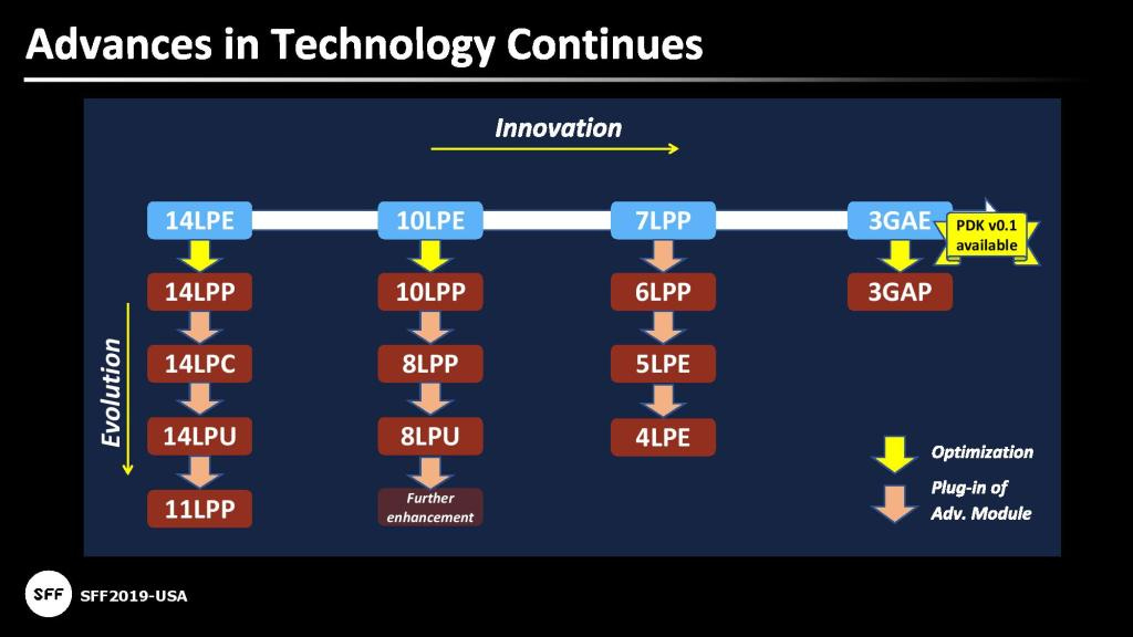
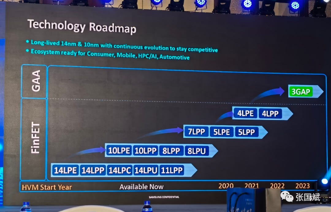
Samsung has reacted to delays in the 3GAE node by inserting a new process technology into their roadmap. The 4LPP node is a new node that is outside the 7nm family. This technology will be showcased in various mobile and radio products from Qualcomm and Samsung. One Qualcomm’s most exciting products in the network infrastructure category, FSM200 was written about here.
The current 5LPE node being succeeded by 5LPP (previously 4LPE) and 4LPP points to further delays for 3GAE. All signs would point to early 2023 for the 3GAE node, even from the most pessimistic industry followers. Samsung’s largest customer, Qualcomm would be first in line to use these technologies alongside Samsung's internally developed chips.
Dr. Chidi Chidambaram is the VP of Engineering and leads the company's process technology and foundry engineering team. He would have direct and intimate knowledge with foundry process roadmaps. He recently spoke at an event by Applied Materials, a critical semiconductor capital equipment provider. At this event, he was asked about the productization timelines for gate all around transistor technology.
“I think you know, ‘24, ‘23 productions. The earliest could be ‘23, but ‘24 production is reasonable, I think”
Dr. Chidi Chidambaram
Dr. Chidi Chidambaram is likely under NDAs for process roadmaps which would explain why he had to be vague. His teams would have directly gone through the failure that was “first customer tape outs in 2020” for the 3GAE node that Samsung loudly proclaimed in 2019. They also have evaluated both TSMC and Samsung for 2022 and 2023 designs. His teams would be in charge of making the decisions on which process technology to utilize for these designs. He seems to be hedging the bet that 2023 is possible, but 2024 is the most reasonable timeline.
This lines up with how Samsung has launched process nodes in the past. For example, with the 14nm, 10nm, and especially 7nm launches, their flagship Exynos line started on the node at low volumes at least 6 months before any foundry offerings came to market.
Given these comments, the best-case scenario is that in the 2nd half of 2023 could potentially see a low volume 3nm based Exynos. In the most optimistic scenario that would mean 3GAE would be a 2024 foundry process node!
This would be a similar time frame to TSMC’s 2nm process node which will utilize gate all around transistor architecture, likely in 2024. While Samsung has focused on a moonshot goal of achieving gate all around transistors, TSMC focused on multiple avenues of scaling such as the usage of cobalt in contacts and interconnects, germanium doped channels, in-house pellicles for EUV, and multi-patterning with EUV. All the while, it looks like they will commercialize a denser gate all around process node in the same time frame.
Samsung and Intel continue to slip further behind TSMC in leading edge technology. Will they ever be able to catch up?
The following edit is an after the original publishing, but we felt it was important to update that Samsung has officially delayed to 2023.
This article was originally published on SemiAnalysis on June 29th 2021.
Clients and employees of SemiAnalysis may hold positions in companies referenced in this article.


Dylan, no where in the article confirms what you suggest in the title and the premise of your speculation such as "Fast-forward to 2021 and there are no tape outs" is factually incorrect since Synopsys did confirm tapeout of 3nm silicon by Samsung Foundry. Are you bothered to edit your article or scrap it all togther?
For Fred Chen & Daniel Nenni, could you at least care enough to check facts before you post this kind of article as an "interesting" read & upvote it as if they were factually correct on your forum?
I understand Nenni is biased for one reason and others, but if you are intended to continue questioning the "trust" issue of Samsung Foundry, you shouldn't be the one who creates the very perception by spreading misinformation.