Tesla Dojo - Unique Packaging and Chip Design Allow An Order Magnitude Advantage Over Competing AI Hardware
Tesla hosted their AI Day and revealed the innerworkings of their software and hardware infrastructure. Part of this reveal was the previously teased Dojo AI training chip. Tesla claims their D1 Dojo chip has a GPU level compute, CPU level flexibility, with networking switch IO. A few weeks ago, we speculated on the packaging of this system being a TSMC Integrated Fan Out System on Wafer (InFO_SoW). We explained the benefits of this type of packaging alongside the cooling and power consumption involved with this huge scale up training chip. Additionally, we estimated that this package would outperform Nvidia systems in performance. All of this seemed to be valid speculation based on the reveal. Today we will dive more into the semiconductor specifics of the reveal.
Before we get ahead of ourselves on the meaty hardware, let’s talk about the evaluation infrastructure. Tesla constantly retrains and improves their neural networks. They evaluate any code change to see if there is an improvement. There are thousands of the same chip that is deployed in cars, in servers. They run millions of evaluations a week.
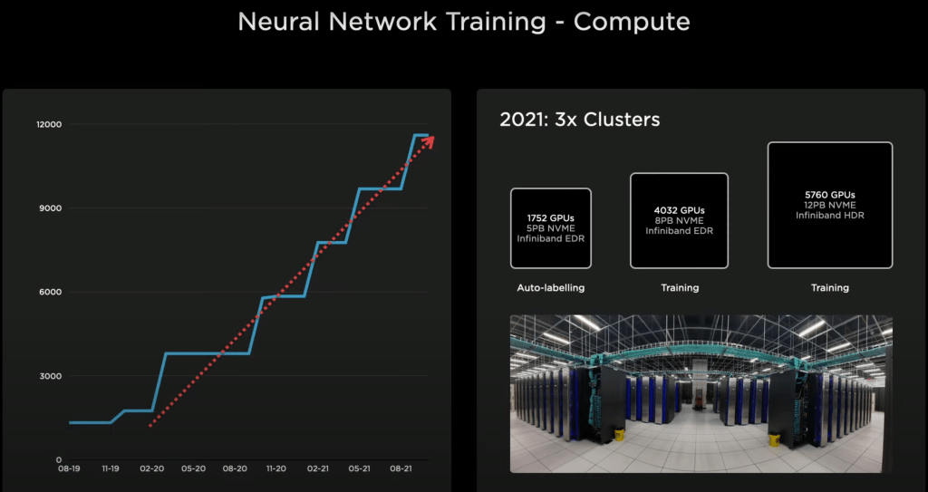
Tesla has been expanding the size of their GPU clusters for years. Their current training cluster would be the 5th largest supercomputer if Tesla stopped all real workloads, ran Linpack, and submitted it to the Top500 list. This scaling of performance is not enough for Tesla and their ambitions, so they set out on developing their own chip a few years ago, project Dojo. Tesla needed more performance to enable even larger and more complex neural networks in a power efficient and cost-effective manner.
Tesla’s architectural solution was a distributed compute architecture. As we listened to their details, this architecture seems very similar to Cerberus. We analyzed the Cerebras Wafer Scale Engine and its architecture here. Every AI training architecture is a laid out in this manner, but the details of the compute elements, the network, and fabric vary widely. The biggest problem with these types of networks is scaling up bandwidth and retaining low latencies. In order to scale to larger networks, Tesla focused on these latter two especially. This influenced every part of their design from the chip fabrics to packaging.
The functional unit was designed to be traversable with 1 clock cycle, but large enough that synchronization overhead and software do not dominate the problem. As such they arrive at a design almost exactly like Cerebras. A mesh of individual units connected by a high-speed fabric which is routes communications between functional units in 1 clock. Each individual unit has a large 1.25MB SRAM scratchpad and multiple superscalar CPU cores with SIMD capabilities and matrix multiply units supporting all common data types. Additionally, they introduce a new data type called CFP8, configurable floating point 8. Each unit is capable of 1TFlop of BF16 or CFP8, 64GFlops FP32, and 512GB/s of bandwidth in each direction.
The CPU is no slouch, it is 4 wide with 2 wide on vector pipelines. Each core can host 4 threads to maximize utilization. Unfortunately Tesla went with a custom ISA rather than building on top open source ISA’s like RISC V. This custom ISA introduces instructions for transposes, gathers, broadcasts, and link traversals.
A full chip of these 354 functional units reaches 362 TFlops of BF16 or CFP8 and 22.6 TFlops of FP32. It is a total of 645mm^2 and 50 billion transistors. Each chip has a breathtaking 400W TDP. This means power density is higher than most configurations of the Nvidia A100 GPU. Interestingly, Tesla achieves an effective transistor density of 77.5 million transistors per mm^2. This is higher than every other high-performance chip, and only beaten by mobile chips and the Apple M1.
Another interesting aspect of the base functional unit is the NOC router. It scales intra and inter chip in a very similar manner to Tenstorrent. Linked is our analysis of that architecture. It’s no surprise that Tesla is arriving at a similar architecture as other well regarded AI startups. Tenstorrent is very geared to scale out training, and Tesla was focusing on this aspect heavily.
On chip, Tesla has a breathtaking 10TBps of directional bandwidth, but this number isn’t that meaningful in actual workloads. One huge advantage Tesla has over Tenstorrent is the bandwidth between chips is significantly higher. They have 576 SerDes at 112GTs. This yields a total of 64Tb/s or 8TB/s of bandwidth.
We are not sure where Tesla is getting their claim of 4TB/s off each edge, it is more likely that number off the X and that number off the Y axis. Never mind the confusing slide, the bandwidth this chip has is insane. The highest known external bandwidth chips currently are state of the are 32Tb/s networking switch chips. Tesla was able to double this with huge amounts of SerDes and advanced packaging.
Tesla connects the compute plane of Dojo chips to interface processors which connect to host systems with PCIe 4.0. These interface processors also enable higher radix network connections that supplement the existing compute plane mesh.
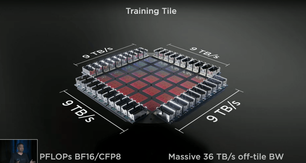
25 D1 chips are packaged as a “fan out wafer process” called a training tile. Tesla didn’t confirm that this packaging is TSMC’s integrated fan out system on wafer (InFO_SoW) like we speculated a few weeks ago, but it seems highly likely given the insane interchip bandwidth and the fact they specifically said fan out wafer.
Tesla developed a proprietary high bandwidth connector that preserves the off chip bandwidth between these tiles. Each tile has an impressive 9 PFlops of BF16/CFP8 and 36 TB/s of off-tile bandwidth. This far surpasses the off-wafer bandwidth of Cerebras, and enables the Tesla system to scale out better than even scale out designs such as the Tenstorrent architecture.
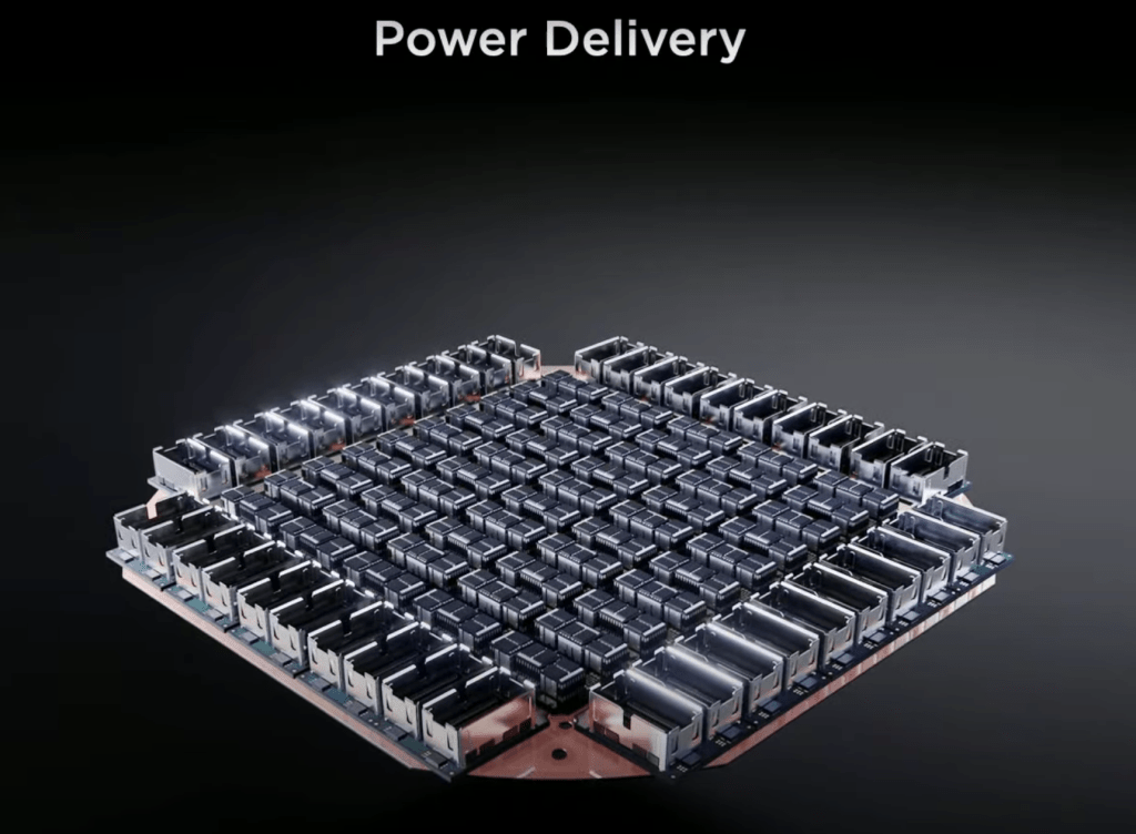
The power delivery is unique, custom, and extremely impressive as well. With so much bandwidth and over 10KW of power consumption on the package, Tesla innovated on power delivery and feeds it vertically. The custom voltage regulator modulator is reflowed directly onto the fan out wafer. Power, thermal, and mechanical are all interfacing directly with the tile.
It appears the total tile is 15KW of power even if the chips themselves are only 10KW total. Power delivery, IO, and wafer wires are drawing a ton of power as well. Power comes in from the bottom while the heat comes out the top. Chips are not the unit of scale for Tesla, the 25 chip tiles are. This tile far surpasses anything from Nvidia, Graphcore, Cerebras, Groq, Tenstorrent, SambaNova, or any other AI training geared start up in per unit performance and scale up capabilities.
All of this seems like far out technology, but Tesla claims they already have tiles running at 2 GHz on real AI networks in their labs.
The next step up to scaling to thousands of chips is the server level. Dojo is scaled up to 2 by 3 tile configs and there are two of these configurations in a server cabinet. For those counting at home, there are 12 total tiles per cabinet for a total of 108 PFlops per cabinet. Over 100,000 functional units, 400,000 custom cores, and 132GB of SRAM per server cabinet is mind blowing numbers.
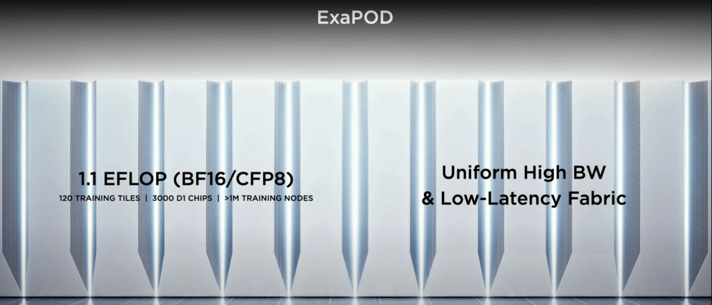
Tesla keeps scaling up further beyond the cabinet level in their mesh. There is no breakdown of bandwidth between chips. It is one homogenous mesh of chips with insane amounts of bandwidth. They plan to scale to 10 cabinets and 1.1 Exaflops. 1,062,000 functional units, 4,248,000 cores, and 1.33TB of SRAM.
My mouth is salivating.
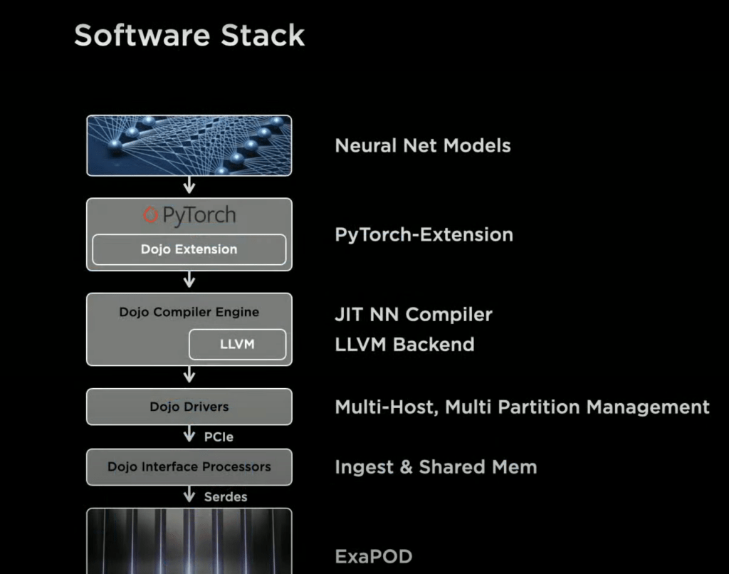
The software aspects are interesting, but we won’t dive too deep into them today. They claim they can subdivide it virtually. They say software can seamlessly scale across the Dojo Processing Units (DPU) no matter the cluster size. The Dojo Compiler can take care of fine-grained parallelism and map networks across the hardware compute planes. It can achieve this with data model graph parallelism, but also do optimizations to reduce memory footprint.
Model parallelism can scale across chip boundaries easily unlocking the next level of AI models with trillions of parameters and beyond. Large batch sizes wouldn’t even be needed. They do not need to rely on handwritten code to run models on this massive cluster.
Rolling it all up, cost equivalent versus Nvidia GPU, Tesla claims they can achieve 4x the performance, 1.3x higher performance per watt, and 5x smaller footprint. Tesla has a TCO advantage that is nearly an order magnitude better than an Nvidia AI solution. If their claims are true, Tesla has 1 upped everyone in the AI hardware and software field. I'm skeptical, but this is also a hardware geek's wet dream. SemiAnalysis is trying to calm down and tell ourselves to wait and see when it is actually deployed in production.
This article was originally published on SemiAnalysis on August 20th 2021.
Clients and employees of SemiAnalysis may hold positions in companies referenced in this article.






now that the Dojo is in production by July 2023, do you have any updates / insights on whether Dojo is working as claimed? thank you