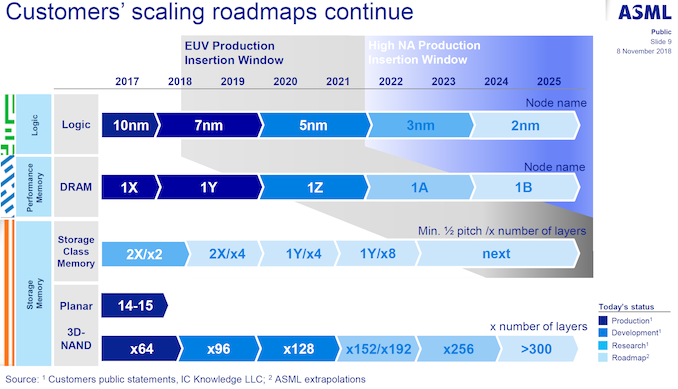
Moore’s law has been the driver of semiconductor capabilities and cost for decades. This phenomenon is still being pushed by the likes of TSMC, Intel, and Samsung in logic, but in DRAM, it is dead. DRAM scaling slowed significantly nearly a decade ago and it is moving at a snail’s pace now. New DRAM nodes are now a tiny fraction of a shrink. Going from 20nm to sub 10nm is going to take at least 5 different incremental node shrinks.
Density has not doubled over even the last 5 years. Despite this, DRAM demand has continued to grow at an incredible pace. This is not a shocker to anyone who follows the semiconductor field.
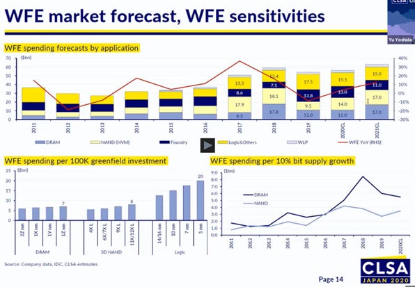
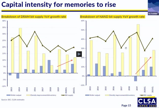
The death of this scaling is what caused previous price spikes. As technology scaling slows, the only way to produce DRAM is with more wafers. It became a very capital-intensive task to increase DRAM bit output when this became true.
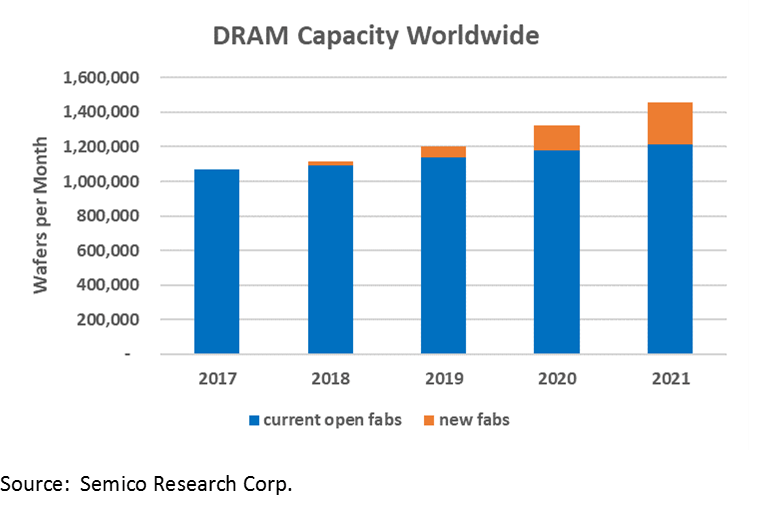
Most of the wafer output increases will be coming from new fabs, as existing clean room space is bursting at the seams. This contrasts from Logic which requires much more clean room space and fab area for node shrinks, despite relatively stable wafer output on the leading edge.
More wafers require additional clean room space and semiconductor capital equipment. This spells great news for the likes of Applied Materials, ASML, Lam Reaseach, KLA-Tencor, and Tokyo Electron. Not all of these companies stand to gain the same and investors should keep this in mind when targeting the DRAM semi capital equipment market.
This article was originally published on SemiAnalysis on May 22nd 2020.
Clients and employees of SemiAnalysis may hold positions in companies referenced in this article.


Joining the Substack crowd, eh? Glad to have you, looking forward to your stuff here!