Lynceus: Inline, Real-time, AI Based Process Control Monitoring That Can Reduce Inspection & Metrology Capex
Lowers inspection and metrology spend with higher yields, demonstrated in high volume fabs
Lynceus is one of the most interesting start-ups out in the semiconductor industry. They aren’t focused on making or designing chips, instead they are focused on software that runs in fabs. Before we dive into their solution, we want to provide some background. Most fabs use various inhouse and external software’s across their fabs. A player like PDF Solutions might provide the database and process solution for tying everything together, various tool companies will provide software for their own tools, and software from the leading inspection and metrology providers such as KLA, Onto, and Nova Measuring Instruments will help identify defects.
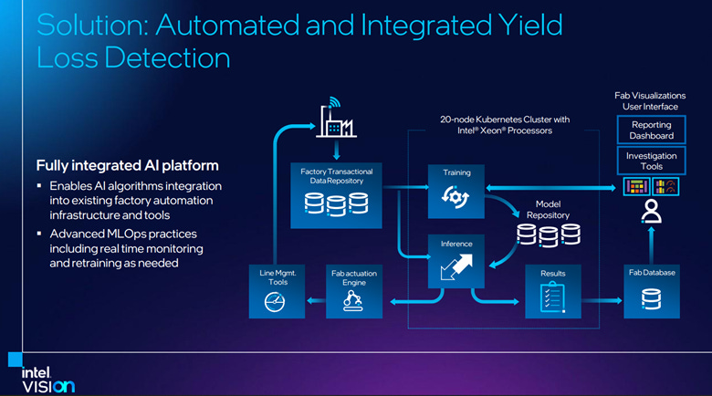
At the end of the day, most software is largely up to the fabs to figure out. Most fabs have very custom flows for determining what data is important, how to act on that data, and how they should constantly tweak their process. Intel has stated they get terabytes of data per wafer produced, but it would be practically impossible to store or analyze it all with classical methods. Despite the volume of data, fabs need to be able to rapidly determine where there are defects, what the cause is, and how to mitigate them.
Data must be constantly monitored and analyzed to determine if a tool is out of spec. Any issues must be caught rapidly or dozens, hundreds, or even thousands of wafers will be ruined. For example, in 2019, TSMC lost over $550M of in-production wafers due to an unidentified issue that persisted inside just 1 fab for less than 1 quarter. At the same time, every inspection or test done on a wafer is floorspace, cycle time, and cost that isn’t advancing the actual manufacture of a chip. The age-old adage of measure twice, cut once is great except that it would be completely uneconomical if that was implemented in semiconductor manufacturing.
As the industry continues to increase complexity, the expectation is that yields still remain excellent. This is an incredibly difficult problem as each successive node adds ~35%+ more process complexity. When leading edge processes measure in the thousands of processes steps, errors can start to stack up quickly. Industrial firms love to talk up "Six Sigma", but that isn’t enough for semiconductor manufacturing. Let’s take a hypothetical process with 2,000 process steps. Even if each step is 6 sigmas in terms of defects per cm2. Then the D0 (industry term for defect rate per cm2) would end up being 0.678. For those unfamiliar, even with a smaller die size like a smartphone chip, more than half your product would be defective.
Any large fab will have at least 1 tool are down for maintenance. A single valve or other parameter of a etch or deposition chamber is just slightly out of spec. It may be running too hot or too cool, it may be operating at the wrong pressure, or the flow rate of a precursor chemical may be out of spec. More often, these issues are even more latent and hard to diagnose than reading a simple sensor. The amount of data coming out the plant is so large that not everything can be analyzed either. There is a constant tradeoff between cost, capacity, yield, time to manufacture, and the quality of product.
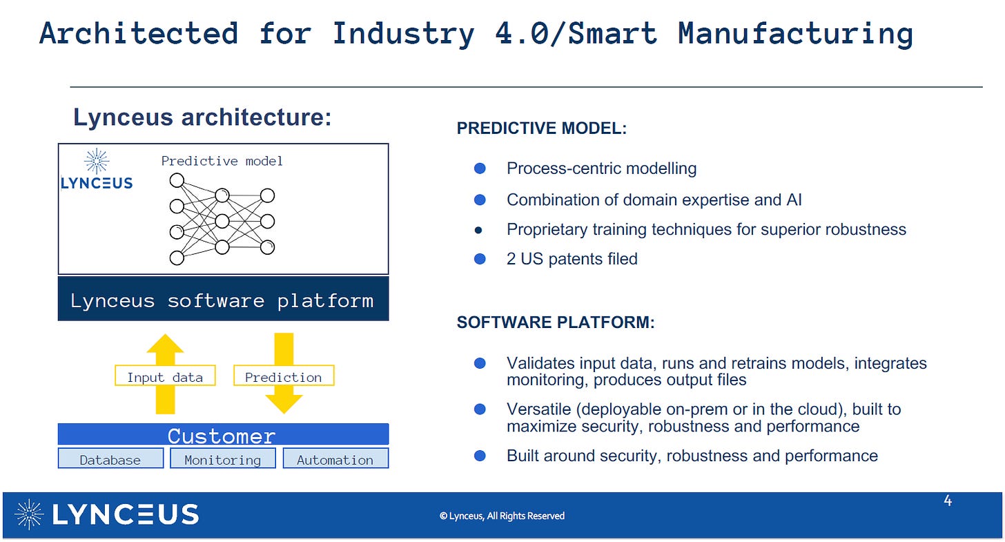
This is where Lynceus comes in. They take data generated from wafer fabrication tools, existing data a fab has on their high-volume manufacturing lines, and build in real-time process control. All data would be fed into various AI models, and they can help identify issues for process and yield engineers. More rapid root cause analysis would help direct the fab’s engineers on critical problems and not waste time on non-issues, increasing engineer efficiency. Another big advantage is that they could start to reduce the amount of inspection and metrology done to optimize the amount of capex and floorspace dedicated to those types of tools that do not advance the manufacturing of a wafer.
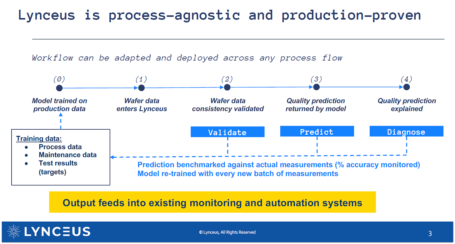
Lynceus is completely process-agnostic, and they are inside fabs generating revenue already. Tool maintenance data, test result data, and FDC data would help train the model. The model can be further tuned for specific processes or even chip designs. As data comes out of an etch, deposition, or other tool chambers, there is a prediction and diagnoses sent. The model is constantly validated and improved.
Their software and models can run in the cloud or on-premises depending on what a fab’s security demand. It is able to plug directly into a fabs existing custom flow and keep the data ownership with that fab.
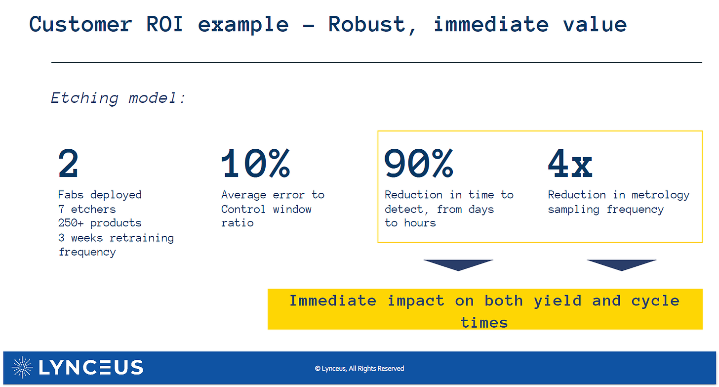
The models are often per process step or module of the process. They are running in production in 2 high volume fabs today with some of these processes. The results are astounding with a 90% reduction in time to detect a defect from 4 days to 3 hours. Furthermore, they were able to achieve a 4x reduction in metrology and inspection sampling frequency. This is a huge boost to yield, cost, and cycle time.
Lynceus’s manufacturing quality prediction software is designed to predict the result of quality tests for each product on the production line. The company's software provides manufacturers with quality predictions in real-time by utilizing AI-based technology to calculate the probability of products passing the quality test, allowing clients to adjust their processes before the defects materialize.
Lynceus can help a fab get more good dies per wafer, lower their cost of goods sold, and achieve higher gross margins. While some larger advanced fabs such as Intel and TSMC are doing similar work for internal use only, most fabs have not implemented models as sophisticated as Lynceus. They are primarily targeting automotive involved fabs as an initial market as there are a large amount of regulatory, test, and quality validation metrics. Once proved here, they can spread further to markets.
As a side node, we have enjoyed being able work with David Meyer, CEO and co-founder of Lynceus as well as the rest of the Lynceus team as they spread their wings and grow into more fabs.


Hi, Dylan.
My mail vlady_kaplan@yahoo.com
Link to the company page https://lvtailoring.webs.com/
and LinkedIn profile https://www.linkedin.com/company/lvtailoring/?viewAsMember=true
and you could look for me at LinkedIn at https://www.linkedin.com/in/lvtailoring/
You could chat if you want, thanks
Well - kind a close call for me - doing same thing with CDSEM Metrology.
Check my company profile - https://lvtailoring.webs.com/ - tons of money could be saved on redefining SW without HW changes