GlobalFoundries is still a leading-edge foundry for semiconductor manufacturing. There is a divergence in the usage of this terminology with companies such as TSMC, Samsung, and Intel chasing the technical definitions of Moore’s Law while ignoring all cost scaling benefits. Many people will erroneously claim GlobalFoundries dropped out the leading-edge race because they stopped their 7nm node development. Despite this being the primary form of leading-edge manufacturing in semiconductors, it’s not the only one. GlobalFoundries is pushing the bleeding edge of manufacturing in other ways that are arguably just as important: silicon photonics, usage of materials such as silicon nitride and gallium nitride for wired and wireless communications, 3D integration, heterogenous integration, and fully depleted silicon on insulator technologies (FD-SOI). Much of this leadership technology comes from the acquisition of IBM’s semiconductor manufacturing business, partnerships with firms in the US defense industry, and subsequent R&D investments built upon this.
GlobalFoundries offers the highest volume and most advanced FD-SOI platform with their 22FDX and upcoming 12FDX process technologies. They will also be a leader in 5G and 6G wireless radio applications with these nodes and their partnership with Raytheon Technologies for Gallium Nitride On Silicon.
GlobalFoundries have demonstrated 3D manufacturing with some of the highest level of integration in the industry. In combination with Arm, GlobalFoundries has publicly demonstrated hybrid bonding of multiple dies with a tighter pitch than any other competitor has with logic nodes. They are utilizing 5.76um copper through silicon vias (TSVs) and can maintain the same clock domain across both chips. These chiplets are made completely transparent and act as a single chip despite being multiple.
TSMC is pushing hybrid bonding mass production soon, with 9um TSVs, stacking SRAM on AMD CPUs. TSMC has plans to introduce 6um and 4.5um over the coming years. Intel is only discussing <10um pitches for their 3rd generation Foveros technology. Sony who pioneered this technology in CMOS camera sensors is currently at 5um. Furthermore, GlobalFoundries has even 3D stacked silicon photonics chips with standard logic chips, a fete no one else in the industry has achieved.
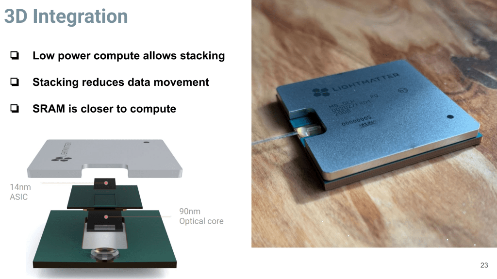
Lightmatter, a silicon photonics AI startup firm that captivated the entire industry at the previous Hot Chips conference, and they utilize GlobalFoundries for manufacturing. GlobalFoundries foundry 90WG process for a silicon photonics computing core, they also utilize a GlobalFoundries standard 14nm foundry process for a control ASIC that also includes stacked SRAM. Lightmatter then utilizes GlobalFoundries leading 3D technologies and capabilities in heterogenous integration to create a single tightly integrated and efficient photonics and logic computing stack.
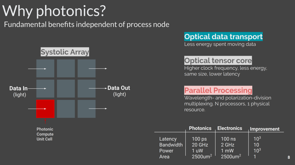
The use of a photonics chiplet allows Lightmatter to achieve multiple orders of magnitude benefit on latency, bandwidth, and power. A tiny fraction of power is spent on transporting data and matrix multiply computations, both of these are very big bottlenecks for AI compute.
The photonics core itself is not a static element. Despite being a silicon photonics process, it is highly reconfigurable which is a stark contrast to other silicon photonics attempts in the industry. It can have its weights reconfigured rapidly. Networks can be tweaked or changed all together. Despite being reconfigurable, the laser input can remain exceptionally low power. The GlobalFoundries 90WG process node ensures there are minimal losses as light bounces around the photonics core and computes.
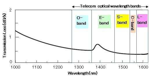
GlobalFoundries currently offers the most advanced silicon photonics foundry services with their 90 Wave Guide (WG) technology. This technology is actively used within datacenter interconnects, 5G remote radio heads, and telecom. Most of the volume is using 1310nm wavelength light for inside the datacenter and long range at 1550nm wavelength light. They are rapidly seeing advances in other areas such as photonic computing, ToF sensors, Lidar, and aeronautics.
These emerging fields will be targeted by their ramping 45CLO process. This process can address silicon photonics demand not only in the O band, but also the C and L band. 90WG is run out of their Fab 9 and 45CLO is run out of much larger Fab 10. The 45CLO process is also a silicon on insulator technology.
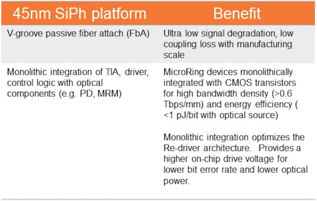
GlobalFoundries 45CLO processes differs from other foundry photonics ICs processes in two ways. It is the only foundry process capable of C band, L band, and O band. Furthermore, they can integrate the active and passive components on a single die. The linear driver, re-driver, and TIAs can now be on the same chip as the optical components such as the photo detector and modulator.
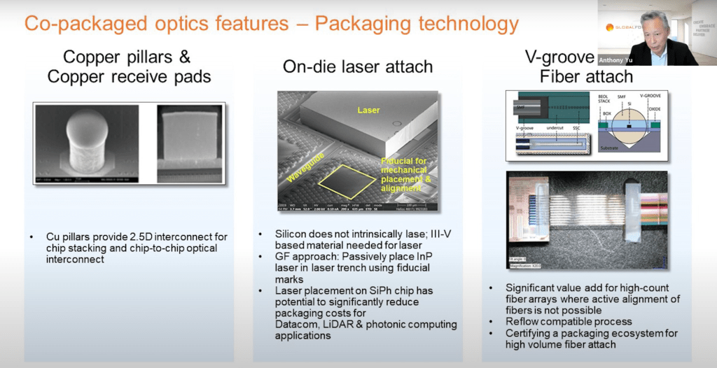
GlobalFoudries has a variety of elements that are supported by the public EDA vendors such as a variety modulator, waveguides made of silicon or silicon nitride, polarization splitters and rotators, passive fiber attach, direct laser attach, and copper pillar and receiver pads. These standardized tools and blocks will allow many fabless companies to easily design and build silicon photonics chips for the everchanging demands of the market.
GlobalFoundries recognizes there is a completely different skillset to produce a chip using electrons vs a chip using photons. There is a complete retooling and change in development practices that must be done. They are fully embracing the change while others in the field have attention split in many directions. This singular focus is allowing GlobalFoundries to become a front runner in emerging leading-edge applications.
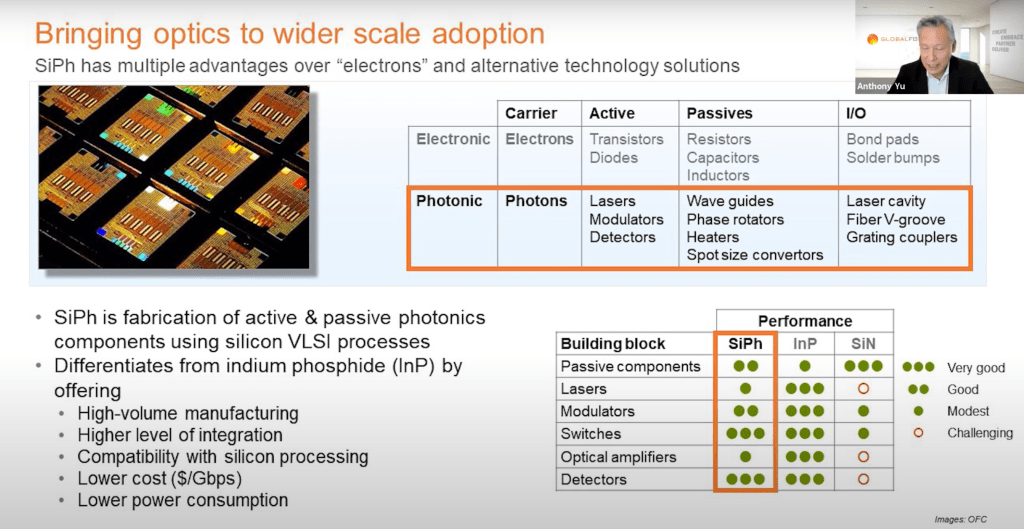
GlobalFoundries is choosing to leverage their expertise in silicon rather than try to entirely shift the whole industry to more exotic materials. Silicon is an indirect band gap material and doesn’t have the same properties as indium phosphide for many photonics applications. There are many negatives for a silicon-based solution for photonics such as in lasers, modulators, and amplifiers. The benefits of using silicon far outstrip the negatives. GlobalFoundries is leveraging 300mm wafer production techniques and the scale of the silicon industry to drive integration of active and passive components onto a single wafer leading to tremendous cost advantages. GlobalFoundries at the same time is offering the ability to integrate these other materials such as Silicon Nitride (SiN) wave guides and Indium Phosphide (InP) lasers with advanced manufacturing and packaging techniques.
Alongside the 45CLO process, GlobalFoundries will be bringing differentiated packaging technologies. These technologies allow them to utilize heterogenous 3D integration with classical logic processes such as the Lightmatter chip shown above. They can bond indium phosphide lasers, saving space, power, and cost versus external lasers. Lastly, they are offering a passive fiber attach process which slides individual fibers into etched v-grooves which directs them into wave guides. This allows higher fiber counts and therefore higher bandwidth densities. In addition to bandwidth density, there are also advantages in complexity of integration and cost.
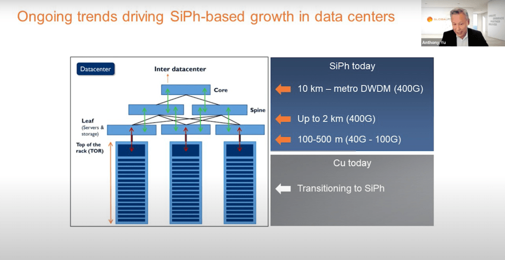
Currently most silicon photonics usage is in optical transceivers in which GlobalFoundries is a leader. 400G technologies are being deployed at scale, and early 800G technologies are starting to crop up. The explosion of data traffic within and out of datacenters is causing intra-rack communications to be disrupted. Currently within a datacenter rack, most communications are currently done through short range copper cables. Copper cables can no longer keep up with scaling demands, and optical fibers driven by SiPh are the only path forward. Even chip to chip interconnects will need to shift to optical in the near-term future or else the percentage of power used for I/O will eat the majority of a package power budget.
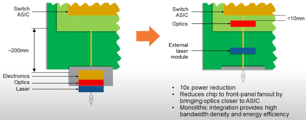
The next wave of high-volume photonics beyond optical transceivers will be co-packaged optics. The left shows the current model with optical transceivers, and the right shows with co-packaging. The electronic, optical, and lasers components are all currently placed a large distance away from the switch ASIC. As we continue to scale in bandwidth demands, this will limit scaling and increase power consumption. Integrating the electronics, optics into a single monolithic chip while bringing it closer to the switch ASIC will drive massive power consumption savings.
Rolling everything up, the largest benefit is your bandwidth density skyrockets. The 45CLO process is capable of greater than 0.6Tbps/mm^2. Power per bit is also an order magnitude better than copper solutions at less than 1pj/bit. GlobalFoundries has customers working on products capable of transmitting 16 different wavelengths of light over a single fiber with a single monolithic chip. An array this complicated previously would have taken dozens of integrated circuits, TIAs, discrete lasers, and independent re-drivers for each wavelength of light. In addition to power and cost, this level of integration also brings a 3-order magnitude benefit on error rates.
While GlobalFoundries has given up on chasing Moore’s law, they have not stopped being a leading-edge foundry. They continue to push the bleeding edge of technology in many other ways. While others focus on generational density and power improvements in computing with electrons in traditional logic process technologies while ignoring, GlobalFoundries is attacking industry wide scaling problems. Their fully depleted silicon on insulator and gallium nitride on silicon technologies are at the forefront of high efficiency and performance radio technologies with the capabilities to drive higher performance and tolerate higher heat and power requirements. Their silicon photonics technologies are the start of a paradigm shift by changing the core element of computers and wired communications from electrons to photons. Their 3D and heterogenous integration expertise allow the combination normal logic, low power FDX, radio optimized, photonics, InP, and SiN technologies to all be integrated into a single innovative solution that utilizes the best technologies for application demands. Due to this advanced technology, Global Foundries is a leading-edge foundry that beats out others such as TSMC, Intel, and Samsung.
This article was originally published on SemiAnalysis on June 21st 2021.
Clients and employees of SemiAnalysis may hold positions in companies referenced in this article.






Dylan - this was a really helpful write-up. As I'm less familiar with the semiconductor business model - I'm curious if you have any further perspective on the 'public EDA vendors' you reference that design chips without fabs for someone like Global Foundries. Are there any successful case studies you could give of companies that have done this that I could explore further?
I guess my ultimate question is trying to determine how much of a moat and platform these vendors have once they get placed into a fab like Global Foundries. For example, going from a no revenue R&D business, to getting a fab agreement, to additional new applications. Does their product offering become commoditized as everyone races to reach their level or is it pretty defensible once you get the fab agreement given how tough it is to break into the production process? And ultimately what the margin structure of these vendors could look like over time.
I know that's an abstract question, but any direction you could point me in would be greatly appreciated. Or happy to chat offline if that's easier.
Thanks!