Ayar Labs | Co-packaged Optics Revolution | The Most Promising Hardware Startup With Wins At HPE And Nvidia?
Ayar Labs is one of the most promising semiconductor startups in the semiconductor world. They were founded in 2015 with a team of many leading technologist from Intel, IBM, Micron, Penguin, MIT, Berkley, and Stanford. Ayar Labs saw one of the most fundamental problems in 2015 and started engineering a solution from the ground up. This is in stark contrast to most hardware startups which are attempting to focus on niches without a true competitive advantage or groundbreaking approach (most AI startups). In this article, we will discuss Ayar Labs funding, the core problem they are solving, and do a deep dive on their technology offering.
Last year, Ayar Labs disclosed that they had a design win with over 5000 units for a custom AI machine, but they have progressed nicely since then. The most recent announcement was that Ayar Labs raised $130M. A startup raising capital is usually something you can ignore, but the way Ayar did it is quite interesting. Some typical funds have given money, but we hear Ayar Labs has intentionally kept their valuations in check by rejecting more money from these money managers.
Pushing away hungry VCs was a smart move given even most successful hardware startups have had valuations peak in the $1B to $2B range. The good ones get acquired there, the bad ones end up having down rounds or fooling people into a higher valuation that never pan out. There’s a lot more we can talk on the topic of private semiconductor fund raising, timing, and investing, but we will save that for another day.
Ayar Labs has instead seemingly focused on strategic investors who can also be partners. In the past, these included big names such as GlobalFoundries, Intel, Lockheed Martin, Applied Materials, and Dowing. The most recent $130M round also brings Nvidia and HPE into the fold. We believe most of these strategic investors came with at least a little bit of technology know how or partnership.
For example, GlobalFoundries was involved in the seed round. We have described them as the leading silicon photonics foundry in the past, and they manufacture on the Ayar Labs Photonics IC on the GFS 45CLO process node. Intel was the first user of the Ayar Labs co-packaged photonics tile with FPGAs, which helped Ayar Labs proof of concept their solution. HPE is working with Ayar Labs on the next generation high performance computer interconnect solution that builds on top of Slingshot and allows for disaggregated server design. While Nvidia has not confirmed their plans we will discuss their potential plans with Ayar Labs later in the article.
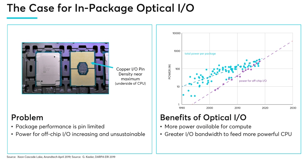
First let’s start off with defining the problem Ayar Labs set out to tackle and why their solution is so ingenious. Input and output (IO) have been the limiting factors for computing. Most the time processors are waiting for data, not actually computing. We described this thoroughly in part 1 of our advanced packaging series, but as a short refresher, the number of pads were data can be input and output out of a semiconductor package has risen very slowly relative to computing data demands. As such the industry has turned to narrower and very high-speed methodologies for the IO of data. Unfortunately, the data rates have also not been able to keep up, and the power consumed by IO has risen disproportionately. IO and data movement power is the primary driver of power increases in server chips. This rate of increase in power consumption is unsustainable and is a tremendous source of inefficiency in computing.
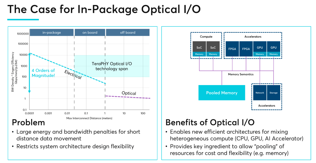
Ayar Labs set out to break this paradigm. Rather than being limited by IO density issues, data rate scaling, and power inefficiencies of electrical package to package interconnects, the goal was to place optical communications directly onto the package. Ayar Labs main point is that Optical IO is more efficient than current electrical regime in the 1cm to 10cm transmission range. The best way to break the problem of ballooning power with data movement is to switch to optical any time you transfer data beyond this distance.
We should build the biggest chips we can. Then we connect them together. The reason for that is because it’s sensible. That’s why chips got bigger and bigger over time. They’re not getting smaller over time. They’re getting bigger. The reason for that is because larger chips benefit from the high energy efficiency of the wires that are on chip. No matter how energy-efficient a chip-to-chip SerDes is, it’s never going to be as energy-efficient as a wire on the chip. It’s just one little tiny thread of wire. We would like to make the chips as big as we can, and then connect them together. We call that superchips.
Do I believe in chiplets? In the future there will be little tiny things you can connect directly into our chips, and as a result, a customer could do a semi-custom chip with just a little engineering effort, connect it into ours, and differentiate it in their data center in their own special way. Nobody wants to spend $100 million to differentiate. They’d love to spend $10 million to differentiate while leveraging off someone else’s $100 million. NVLink chip-to-chip, and in the future UCIe, are going to bring a lot of those exciting opportunities in the future.
Jensen Huang, Nvidia Founder and CEO
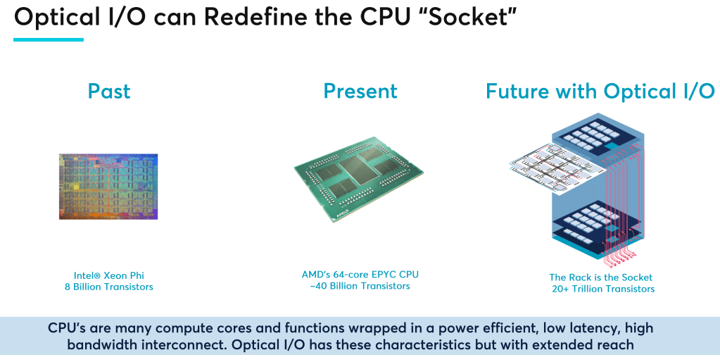
Currently we have strict hierarchies of compute, memory, accelerators, and networking all within fairly small server boxes. The barrier between a server and outside of it is a very expensive barrier to cross in terms of efficiency. Companies are rushing to make packages larger and larger to continue to scale up performance and reduce costly communications with the external world, but this is extremely costly as you move to exotic packaging technologies which enable these large packages. As such, AMD, Intel, Nvidia, and others temper package size increases. Even if packaging was free, problem sets in high performance computing and AI are far too large to fit in even wafer scale packages such as Cerebras or System on Wafer packages such as Tesla’s Dojo AI training architecture.
If the paradigm of power cost for data movement was equalized between package to package in the same server versus in other servers and server racks, the entire system architecture of server design would shift. The best solution for high performance applications would stop being many racks of independent servers interconnected to act as one, but instead would be a massive pool of highly composable groups of memory, CPUs, networking, and accelerators. This sea of compute and memory would all be relatively close to each other on a latency perspective while also not incurring huge power penalties.
Under this lens, it is obvious why HPE, the largest supercomputer contractor in the world, and Nvidia, the company who has over 95% accelerators share in high performance computing, are strategic investors. They need to use this technology for the next generation of high performance computing architecture. Nvidia seems a bit odd as a strategic investor given they have over a hundred people focused on optical based communications. Nvidia has also done multiple acquisitions in the space, but this just speaks to Ayar’s technical capabilities here. We imagine the deal could be some sort of licensing scheme or short term external Band-Aid solution.
Moving to co-packaged optics has many benefits which may not be immediately obvious. Data doesn’t need to be sent from the processor to a networking card, and through expensive optical transceivers. The processor itself can also save a lot of cost by not having to dedicate as much die area to large high-speed electrical SerDes. Given Ayar Labs has joined the open UCIe standard, we believe their chiplets will use this protocol as the base layer to interface with external firms chips. UCIe supports many packaging options from Intel, ASE, and TSMC. On the processor side, Intel, AMD, Broadcom, Micron, Mediatek, and GUC are part of the consortium. UCIe tremendously lowers the barrier to entry for integrating 3rd party chiplets into packages which in turn should reduce the barrier to entry for Ayar Labs to achieve design wins. Even without UCIe, Ayar Labs explicitly supports high density fan outs, Intel’s EMIB, and other silicon interposer technologies.
The beauty of the UCIe and Ayar Labs solutions are that they are protocol agnostic. The TeraPHY chiplet could carry high latency Ethernet if they want, but the real value is that it can carry PCIe 5.0, CXL 2.0, or potentially even custom protocols such as Nvidia’s NVLink. Nvidia’s NVLink on GPUs and NVSwitch seems like the perfect application given Hopper NVLink fabric scales up to 256 GPUs across multiple racks. Nvidia will want to increase this number further with the next generation. Power budgets are clearly ballooning with the H100 SXM5 GPU and NVSwitch both increasing quite sizably gen over gen.
Ayar Labs claims lower than 5pj per bit transferred. This is roughly 1/3 that of next generation 800G optical transceivers. In most cases the data will also have to pass through a networking switch and more hops through optical transceivers or direct attached copper, so the power difference would be even larger. In cases like these, the Ayar Labs solution could be an order of magnitude more efficient and lower latency compared to these traditional Ethernet solutions.
The current generation TeraPHY is a tiny 75mm2 die which is capable of 2Tbps of IO. The typical 0.2Tbps optical transceiver is a total of ~150mm2. Ayar Labs is using far less silicon than the equivalent IO speeds in pluggable optical transceivers, and this isn’t even accounting for area saved on processor SerDes. We should note that the Ayar Labs figure does not include the external laser, which we will discuss later in this article. The 2Tbps TeraPhy runs through 8 single mode fibers. Many pluggable optical transceivers use multi-mode fibers, so that is a tradeoff. Each single mode fiber utilized by Ayar Labs carries 8 channels of 32Gbps NRZ. This is also more efficient than the more complex PAM4 encoding scheme. NRZ is also lower latency due to the lack of required FEC.
For those keeping track, this means that each TeraPHY chiplet can offer a total of 64 lanes of PCIe 5.0 / CXL. Ayar Labs example is a processor with 4 TeraPHY chiplets, so theoretically that is 256 lanes! Future generations can scale on multiple axis by adding more channels per fiber via more micro-ring modulators, increasing the data rate to 64Gbps, or moving up to more fibers. Given Hyper X topologies are also supported, there can be a network of processors, accelerators, and memory with very high bandwidth and radix.
A few elements make up the secret sauce for Ayar Labs. Most optical chips use mach zehnder modulators to encode data into the light from the laser, but these are very large and therefore they limit the ability to pack many channels densely. Ayar Labs on the other hand is using micro-ring modulators. This type of modulator is far smaller and more efficient. The difference in modulators is the primary reason for the typical transceivers being twice as much silicon while consuming 3x the power per bit transferred versus Ayar Labs TeraPHY.
The issue with micro-ring modulators is that they have been notoriously difficult to yield. This is because even a sub-nanometer variation on the micro-ring structure would change the wavelength outputted when encoding data, or even cause errors during the encoding. Furthermore, beyond the manufacturing difficulties, micro-rings are also extremely temperature sensitive. Ayar Labs claims to have solved this with their manufacturing partner GlobalFoundries. While they didn’t tell us how, we believe it is through intentionally controlling the temperature of the micro-ring modulators. Ayar Labs likely has circuits around each modulator that constantly turn on or off to precisely raise and lower the temperature of the micro-ring modulators to ensure data is encoded to the right wavelength and without errors. This scheme would allow for each modulator to be individually tuned. This scheme would allow for each modulator to be individually tuned.
The other major advantages beyond tighter integration of both the photonics IC and the packaging is by using disaggregated lasers. This is in stark contrast to Intel, who currently has a large cost advantage in the optical transceiver world. Part of Intel’s advantage is due to their integrated bonded lasers. Ayar Labs believes they have an advantage due to reliability concerns. With pluggable optics, reliability concerns are eschewed because you can replace the transceiver, but with co-packaged optics, any unreliability concerns would hamper the capabilities of the entire package.
With Nvidia’s current generation Hopper SXM5 reportedly selling for above $20k, and top end networking switch ASICs at over $40k, hopefully you can see how bad even 99% reliability would be. As such, Ayar is going with an external laser model because lasers are the most likely portion of optics to fail. There is already an open standard called CW-WDM MSA for external lasers. It is already supported by 49 companies and Macom, Sivers Photonics, and Lumentum currently have 3rd party lasers available.
Ayar Lab has demonstrated amazing success and capabilities which make them the most promising hardware startup. They have big wins at companies such as HPE, and the strategic investment from Nvidia is certainly a head turner. They are the furthest along on a co-packaged optics solution and by supporting open standards and many types of packaging they have opened the walls of the dam for potentially revolutionizing the architecture of high-performance computing. Their innovation alongside GlobalFoundries on micro-ring modulators is a huge deal given their reliability claims. This would be an industry first for a high-volume products. Pluggable optics will always have their place, but co-packaged optics have many clear advantages on power, performance, bandwidth density, and even cost.
Clients and employees of SemiAnalysis may hold positions in companies referenced in this article.


do they design in-house serdes or license? should be custom to drive those rings directly I assume...
how far this is from productization as far as cost/reliability goes? few years? is this going to kill AEC?
" HPE, the largest supercomputer contractor in the world"?
Is it really bigger than the biggest Chinese supercomputer contractor?