Semiconductor manufacturing is nearly an alchemy like process of making rocks think. In the process of manufacturing a chip or device, there are constant checks throughout the process of manufacturing, packaging, and assembly. There are a variety of firms in this space for “checking” semiconductors both during and after manufacturing.
One area of “checking” is metrology where firms like KLA-Tencor $KLAC, Nova Measuring $NVMI, Onto $ONTO, and Camtek $CAMT measure the results and potential issues after each process steps involved in the manufacture of semiconductors. FormFactor $FORM, Micronics Japan 6871.JP, and Technoprobe make custom probe cards which make physical contact with wafers to test them after the wafer manufacturing process is completed. Advantest $ATEYY and Teredyne $TER are most well known for their automated test equipment which tests chips after the wafer is diced. Cohu $COHU operates primarily in the handling of these devices but is also involved in testing and contactors. These are general industries these firms operate in, but they do venture out of those boxes to varying degrees.
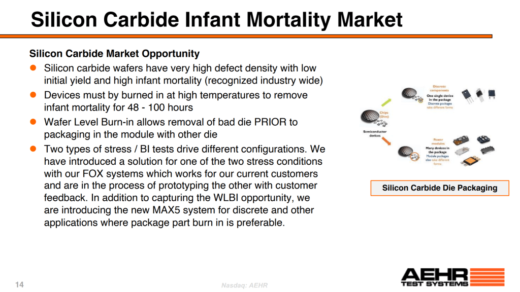
Silicon carbide (SiC) devices are extremely expensive to fabricate and package. Failures in the end markets of electric vehicles, chargers, and energy infrastructure would be catastrophic. These devices may function perfectly fine at normal temperatures, but failures and irregularities will become apparent in the more extreme environments. Due to qualification requirements to operate at very extreme temperatures for long periods of time, there’s no skimping out on testing.
Individual tests can last two to four days per device and the footprint required for testing thousands of devices is astronomical. In a multi-die module, one bad die would cause many good dies to fail. SiC has many defects related to the fragile/brittle crystalline structure, doping related defects, and trench failures. Yield here are especially low relative to other semiconductors, and contribute to about 30% of final device cost. The bathtub curve applies to semiconductors. Mortality rates are very high in the beginning, but exponentially decrease to a steady state. After a long period of low failure rates, they eventually start to rise again.
Aehr operates in an interesting area that is analogous to certain test related sub-segments of Advantest, Teredyne, and Cascade Microtech (FormFactor subsidiary). Aehr’s approach is complexly novel though. Instead of creating tools for testing on the device and module level, they do test at the wafer level. This allows for fewer failed devices to be packaged and for the full test cycle to be shortened. Cycle times are a major limiting factor in SiC device production and Aehr's solution to decrease the cycle times is promising. On Semiconductor $ON is the first hallmark customer for Aehr in SiC, but they are engaged with others.
Aehr has developed the FOX-XP tool for burn-in test for silicon carbide wafers. Each wafer can contain as many as a thousand SiC devices. FOX-XP can test 18 wafers at a time. FOX-XP does this inside the chamber which acts as a highly regulated extreme temperature environment. This can be thought of as an oven, except its capable of dissipating over 18 kW too. The FOX-XP tools cost about $2.5M and must be used with the WaferPak Contactor.
The WaferPak is similar to a probe card, but it also carries the wafer. WaferPaks are considered a consumable and costs around $1.5M. Consumables are products that are used up and have reoccurring revenues rather than large 1 time payments like tools. It has 2048 I/O pins and DPS channels. Each channel has remote voltage and ground sense. Each of these channels can cycle between 1024 voltage levels up to 29V or run as high as 2A. This isn’t quite as capable of fine grained testing and control like a high-end probe card, but it allows some basic testing while operating at in temperature ranges as high as 150 degrees Celsius.
The last piece is the automated FOX-XP WaferPak Aligner which loads and unloads wafers between FOUPs or wafer cassettes and the WaferPak Contactors. WaferPak Aligner's cost less than $1M. The final system automatically loads and unloads wafers, tests them for days, and identifies failed devices. Using wafer level testing vastly reduces footprint dedicated to test for SiC devices. Rather than having many machines that tests many individual devices in parallel for days on end, a single FOX-XP can test 18 wafers each containing many devices. This dramatically increases throughput as over 10,000 individual devices can have an in depth burn-in testing with the use of only a single tool. Costs are reduced as bad devices can be binned away before packaging.
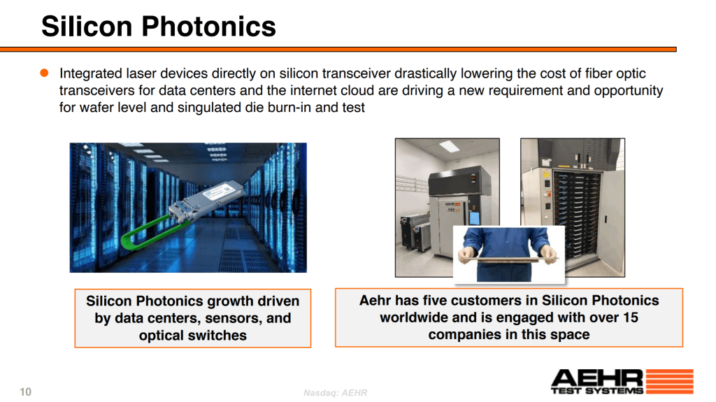
Silicon carbide semiconductors are not the only area moving to wafer level burn-in testing. Silicon photonics is adopting it. Intel is Aehr’s hallmark customer for photonics applications, but they have stated they have 4 other customers in this space. Burn-in is used for the laser in this application. There are indium phosphide lasers that Intel fabricates and then bonds onto each photonics integrated circuit (PIC). Intel's 400G transceivers will contain 4 of these lasers on a PIC and 800G will contain 8.
Each laser is beamed through the PIC and the light stream is encoded with 100 gigabits of data. There must be an extreme degree of precision with these lasers to transfer data reliably without errors. Any change in the laser's operation will throw off the finely tuned system. Lasers have a phenomena that is almost analogous to the bathtub curve of reliability. In initial use, there is a decay and the wavelength of light outputted shifts. Following this the laser stabilizes for its useful life. Intel and other photonics manufacturers burn-in the lasers for the duration of this decay period. Once the wavelengths stop shifting, they can identify failures, and calibrate systems. The next step would be to package the PIC/Laser onto the final transceiver module. The real kicker is with silicon photonics volumes exploading at 400G, 800G, and eventually copackaged photonics.
The physical system is slightly different for photonics applications. Each FOX-XP can hold 9 FOX Die-Pack Carriers. These carriers house up to 1024 individual dies each of which can receives 2 W for the laser to burn-in. This is a total of 18 kW. There is a mobile and sensors angle here as well. VCSEL lasers can be used for optical sensing in markets such as Lidar. These sensors could be used anywhere from cars to the lidar on iPads and AR. There’s a possibility for this to be used to burn-in the lasers in health applications such as with Rockley Photonics.
Aehr has stayed a small for decades, but right now they are entering an inflection point. With the move to 400G, 800G, and co-packaged photonics, the number and quality criteria for lasers will explode. Intel’s silicon photonics volumes will soar and that likely means more Aehr systems. If they can convince the fledgling SiC industry that wafer level burn-in test should be implemented in the test cycle, they can rack up huge wins as volumes begin to boom. The current valuation has Aehr getting quite a few more wins and growth with existing clients. We can't be certain Aehr gets these wins, but it is certainly a company to keep an eye on. The largest SiC players haven’t committed yet, but if they do, the sky is the limit. Wafer level burn-in is too expensive for most mass volume semiconductors, but compound semiconductors and photonics flip that paradigm on its head.
This article was originally published on SemiAnalysis on September 29th 2021.
Clients and employees of SemiAnalysis may hold positions in companies referenced in this article.


Great analysis. Thank you helped me get into the stock. Would you do an update? Things have changed dramatically for the company. Orders are flowing as they have 2 of the 4th larger sliicon carbide manufacturers as client. On semi is their largest customer do you know who is the second one? Is it ST Micro or Infineon? Wolfspeed is building huge factories but is not yet a client. While the stock price has surged I think that the level of profitability as the current low level of sale indicates impressive operating income leverage. Estimates will have to increase materially. Finally what is your thought about the potential of photonics in the data centers. The company seems to believe it could be a huge factor to increase the TAM for the company. Thank you
You guys realize who the end user of ON semi is right? I heard rumors for weeks on who it was and i just about confirmed it today. It is TESLA. yes TESLA.. So i assume more big orders will come its way thru ON semi but i do believe bigger customers are gonna come on line hopefully soon. At 300 millionish market cap i think its got a ways to go